
Perovskite-Based Near-Infrared Photodetectors
Received date: 2023-05-25
Revised date: 2023-08-09
Online published: 2023-09-10
Supported by
National Natural Science Foundation of China(62004058)
Natural Science Foundation of Hebei Province(F20202022)
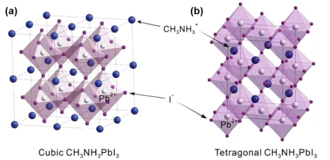
In recent years, organo-metal halide perovskites materials with ABX3 crystal structure have shown promising application prospects in the field of photoelectric detection due to their optical and electrical properties such as adjustable bandgap engineering, high absorption coefficient and long carrier transmission distance. Especially, the hybrid perovskite prepared by pure Sn or Sn/Pb mixed cations have excellent near-infrared photoelectroresponse in the range of 760~1050 nm, showing many advantages such as high sensitivity, low dark current and high detection rate. To further broaden the near-infrared and infrared response wavelength range of perovskite, the researchers explored combining organic materials, crystalline silicon/germanium, Ⅲ-Ⅴ compounds, Ⅳ-Ⅵ compounds, upconversion fluorescent materials as complementary light absorption layers with perovskite to prepare heterostructures to construct wide-spectrum response near-infrared photodetectors. Based on the above research, this paper summarizes the current effective ways to broaden the spectrum range of perovskite photodetectors. At the same time, the future development prospect of perovskite material near infrared photodetector is prospected.
Contents
1 Introduction
2 Basic indicators of photodetectors
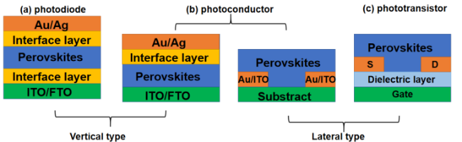
2.1 Device structure and working principle of photodetectors
2.2 Performance parameters of photodetectors
2.3 Strategy of broadening the spectrum response range of perovskites
3 Pb perovskite for near-infrared photodetectors
3.1 Polycrystalline perovskite materials
3.2 Single crystal perovskite materials
4 Narrow band gap Sn and Sn/Pb Mixed Perovskite- Based near-infrared photodetectors
4.1 Sn-based perovskite near-infrared photodetectors
4.2 Sn/Pb mixed perovskite near-infrared photodetectors
5 Perovskite/inorganic heterojunction near-infrared photodetectors
5.1 Silicon and other classic semiconductors
5.2 Graphene
5.3 Transition metal dichalcogenides
5.4 Ⅲ-Ⅴ compounds semiconductors
5.5 Ⅳ-Ⅳ compounds semiconductors
6 Perovskite/organic heterojunction near-infrared photodetectors
7 Perovskite/upconversion material near-infrared photodetectors
8 Application of near-infrared photodetectors
9 Conclusion and outlook

Wenhuan Gao , Jike Ding , Quanxing Ma , Yuqing Su , Hongwei Song , Cong Chen . Perovskite-Based Near-Infrared Photodetectors[J]. Progress in Chemistry, 2024 , 36(2) : 187 -203 . DOI: 10.7536/PC230526
图3 (a) ZnO纳米棒/ MAPbI3 PDs能级匹配图[17];(b) MAPbI3-xClx用于柔性器件示意图[18];(c) MAPbI3纳米晶体 PDs的光电流和响应度[19];(d) MAPbI3单晶照片[21];(e) MAPbI3单晶响应速度曲线[22];(f) MAPbI3单晶空间电荷限制电流测试(SCLC)[23]Fig.3 (a) Energy level matching diagram of ZnO nanorods/ MAPbI3 PDs[17];(b) Schematic diagram of MAPbI3-xClx for flexible devices[18];(c) Photocurrent and responsivity of MAPbI3 nanocrystalline PDs[19];(d) Photographs of MAPbI3 single crystals[21];(e) Response velocity curves of MAPbI3 single crystals [22];(f) MAPbI3 single crystal space charge limiting current test (SCLC)[23] Copyright 2017, American Chemical Society. Copyright 2017, Nature. Copyright 2020, Wiley-VCH. Copyright 2016, Wiley-VCH. Copyright 2018, Elsevier. Copyright 2022, Royal Society of Chemistry. |
表1 常见Sn基和 Sn/Pb基钙钛矿NIR-PDsTable 1 Common Sn and Sn−Pb Perovskite NIR-PDs |
| Perovskite | Wavelength range (nm) | Responsivity (mA·W−1) | Detection rate (Jones) | EQE (%) | LDR (dB) | Response time [trise/tdecay] | Ref. |
|---|---|---|---|---|---|---|---|
| MASnI3 | 300~1000 | 470 | 8.8×10¹⁰ | 1.5 s/0.4 s | 30 | ||
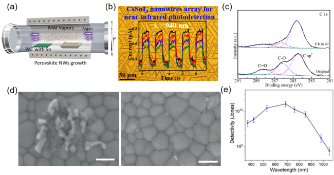
| CsSnI3 | 475~940 | 54 @940 nm | 3.85×10⁵ | 83.8 ms/243 ms | 31 | ||
| CsSnI3 | 400~900 | 257 | 1.5×10¹¹ | 0.35 ms/1.6 ms | 32 | ||
| FASnI3 | 300~1000 | 33 | |||||
| FASnI3 | 300~1000 | 1.1×10⁸ | 1.9×10¹² | 180 s/360 s | 34 | ||
| FASnI3 | 300~1000 | 2×10⁸ @850 nm | 3.2×10¹² | 117 s/206 s | 35 | ||
| PEA0.15FA0.85SnI3 | 450~850 | 0.39 | 8.29 × 10¹¹ | 0.78 μs | 50 | ||
| MA0.975Rb0.025Sn0.65Pb0.35I3 | 300~1100 | 400 @910 nm | >1012 | 110 | 40 ns/468 ns | 38 | |
| MASnxPb1-xI3 | 300~1100 | 200 @940 nm | >1011 | >20% @780-970 nm | 100 | 0.09 μs /2.27 μs | 39 |
| FA0.85Cs0.15Sn0.5Pb0.5I3 | 600~1000 | 530 @940 nm | 6 ×10¹² | ≈80% @ 760-900 nm | 103 | 58.3 ns/0.86 μs | 40 |
| (FASnI3)0.6(MAPbI3)0.4 | 300~1000 | 400 @950 nm | 1.1 × 10¹² | >65% @350-900 nm | 167 | 6.9 μs/9.1 μs | 14 |
| Cs0.05MA0.45FA0.5Pb0.5Sn0.5I3 | 300~1050 | 530 @910 nm | 2.01 × 10¹¹ | 0.035 μs | 41 | ||
| CsPb0.5Sn0.5I3 (5% (PEA)2Pb0.5Sn0.5I4) | 700~900 | 270 @850 nm | 5.42×10¹⁴ | 42 | |||
| MA0.5FA0.5Pb0.5Sn0.5I3 (2.5% (PEA)2Pb0.5Sn0.5I4) | 700~900 | ≈100 @800 nm | ≈1.6 × 10¹² | ≈14% @800 nm | 10 μs /10 μs | 51 | |
| (MAPbI3)0.5(FASnI3)0.5 | 300~1050 | 410 | 2.91×10¹² | >60 @808 nm | 10.9 ms/8.9 ms | 43 | |
| MA0.5FA0.5Pb0.5Sn0.5I3 | 350~1000 | >200 @ 800~950 nm | >1012 | ≈10% @800 nm | 44 | ||
| MA0.3FA0.7Pb0.5Sn0.5I3 | 470~910 | 600 | 1.5 × 10¹² | 85% @850 nm | 45 | ||
| FA0.5MA0.45Cs0.05Pb0.5Sn0.5I3 | 300~1050 | 350 @950 nm | 2.21 × 10¹¹ | 75% @800 nm | 185 | 42.9 ns | 46 |
| Cs0.15FA0.85Pb0.5Sn0.5I3 | 300~1050 | 520 @850 nm | 5.34 × 10¹² | 75% @850 nm | 224 | 39.68 ns | 47 |
| FA0.7MA0.3Sn0.5Pb0.5I3 | 450~900 | 510 | 1.8 × 10¹² | 75.4% @840 nm | 94 ns/97 ns | 48 | |
| FA0.85Cs0.15Sn0.5Pb0.5I3 | 400~900 | 570 | 8.48 × 10¹² | 80 @910 nm | 67.5 ns/0.72 μs | 49 | |
| MASn0.25Pb0.75I3 | 500~900 | 510 | 1.1 × 10¹³ | 192.6 | 52 |
图4 (a) Sn钙钛矿NWs的样品示意图[30] ;(b) CsSnI3钙钛矿PDs上升/下降时间[31];(c) 在空气中暴露6 h后的CsSnI3样品XPS曲线[32];(d) 有无KHQSA修饰的FASnI3薄膜的SEM图像[33];(e) FASnI3/PEDOT:PSS异质结的PDs的探测率曲线[35]Fig.4 (a) Sample schematic of Sn perovskite NWs[30];(b) Rise/fall time of CsSnI3 perovskite PDs[31];(c)XPS curves of CsSnI3 samples after exposure to air for 6 h[32];(d) SEM images of FASnI3 thin films with and without KHQSA modification[33];(e) Detectivity curves of FASnI3/PEDOT:PSS perovskite PDs [35] Copyright 2016, American Chemical Society. Copyright 2019, American Chemical Society. Copyright 2020, Wiley-VCH. Copyright 2019, Wiley-VCH. Copyright 2020, American Chemical Society. |
图5 (a) MASnxPb1-xI3钙钛矿薄膜的带隙(0 < x < 1) [37] ;(b) 有无铷离子掺杂下的钙钛矿薄膜的XRD图像[38] ;(c) 不同结晶时间下钙钛矿薄膜的SEM图像[39];(d) 不同厚度下(FASnI3)0.6(MAPbI3)0.4钙钛矿薄膜的SEM图像[14];(e) 利用PEAI双面钝化Sn/Pb钙钛矿PDs EQE 光谱曲线[41] ;(f) 有无偶氮苯衍生物下PDs的光电流和暗电流J-V曲线[46]Fig.5 (a) Band gap of MASnxPb1-xI3 perovskite films (0 < x < 1)[37] ;(b) XRD images of perovskite films doped with or without rubidium ions[38] ;(c) SEM images of perovskite films at different crystallization times[39];(d) SEM images of (FASnI3)0.6(MAPbI3)0.4 perovskite films with different thicknesses [14];(e) Double-sided passivation of Sn/Pb perovskite PDs EQE spectral curve by PEAI[41] ;(f) Photocurrent and dark current J-V curves of PDs with or without azobenzene derivatives[46] Copyright 2018,Wiley-VCH. Copyright 2018, Wiley-VCH Copyright 2019, American Chemical Society. Copyright 2017, Wiley-VCH. Copyright 2020, Wiley-VCH. Copyright 2021,Elsevier. |
表2 常见Pb基钙钛矿NIR-PDsTable 2 Common Pb Perovskite NIR-PDs |
| Perovskite | Wavelength range (nm) | Responsivity (mA·W−1) | Detection rate (Jones) | EQE (%) | LDR (dB) | Response time [trise/tdecay] (µs) | Ref. |
|---|---|---|---|---|---|---|---|
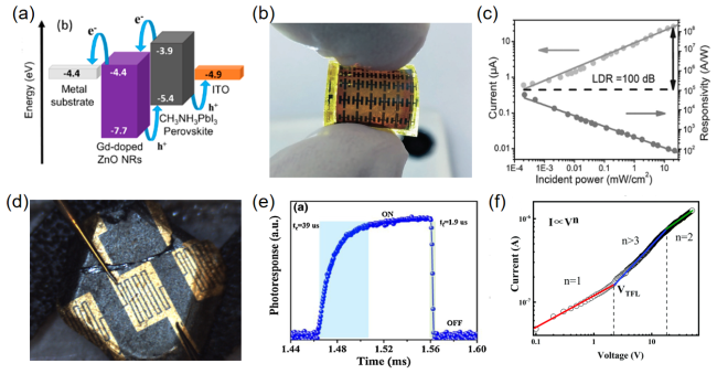
| MAPbI3/Gd-doped ZnO nanorods | 250~1357 | 220 @1357 nm | 9.3×10⁹@1357 nm | 4 × 10⁵ /5 × 105 | 17 | ||
| MAPbI3-xClx | 1012 @1100 nm | 5.6 × 10¹³ @895 nm | 18 | ||||
| MAPbI3 | 400~1064 | 150 @820 nm | 22% @820 nm | 1.2 × 10⁵/8 × 104 | 21 | ||
| MAPbI3 | 400~1000 | 4 × 10³ @800 nm | 600% @800 nm | 39/1.9 | 22 | ||
| CsPbBr3/GeSn | 450~2200 | 4.7 @2200 nm | -/26 | 55 | |||
| Si/MAPbBr3 single crystal | 405~1064 | 5 @1064 nm | 2×10¹⁰ @1064 nm | 0.52/2.44 | 56 | ||
| MAPbI3/Si-NPA | 400~1050 | 8.13 @780 nm | 9.74 × 10¹² @780 nm | 253.3/230.4 | 57 | ||
| MAPbI3-x(SCN)x/Si-NWs | 350~1100 | 1.3 × 10⁴ @800 nm | 1.0 × 10¹³ @800 nm | 22.2/17.6 | 58 | ||
| Cs-doped FAPbI3/Si nanowire array | 300~1200 | 14.86 @850 nm | 2.04 × 10¹⁰ @850 nm | 4/8 | 59 | ||
| PVP-modified MAPbIxCl3-x/Si | 405~988 | ≈1250 @988 nm | ≈5.3 × 10¹¹ @808 nm | ≈275% @808 nm | 44 | 645/560 | 60 |
| Si/MAPbI3 | 300~1150 | 50.9 @815 nm | 2.23 × 10¹² @815 nm | <10% | 1.3×10⁴/1.46× 104 | 61 | |
| MAPbIxCl3-x/Si | 300~1150 | 870 @800 nm | 6 × 10¹² @800 nm | 5×10⁴ /1.5×105 | 62 | ||
| MAPbI3/Si | 400~1200 | 18.4 @970 nm | 1.8 × 10¹² @970 nm | 23.5% | 97 | ||
| graphene/CH3NH3PbI3 | 400~800 | 180 | >1015 | 5×10⁴% | 87 ms/540 ms | 63 | |
| (PEA)2(MA)2Pb3I10/GaAs NWs | 400~800 | 75 | 1.49×10¹¹ | 568 ms/785 ms | 74 | ||
| FA0.85Cs0.15PbI3/PtSe2 | 300~1200 | 117.7 @808 nm | 2.91 × 10¹² @808 nm | 14.9% @808 nm | 0.078/0.060 | 68 | |
| FA0.85Cs0.15PbI3/PtSe2 | 200~1550 | 313 @808 nm | 2.72 × 10¹³ @808 nm | 50% @808 nm | 3.5/4 | 69 | |
| MAPbI3/MoS2 | 500~850 | 1.11×10⁵ @850 nm | 2.39 × 10¹⁰ @850 nm | 6.17×10⁶/4.5× 106 | 71 | ||
| graphene /(PEA)2SnI4/MoS2/ graphene | 300~900 | 121 | 8.09 × 10⁹ | 38.2 | 34 ms/38 ms | 70 | |
| MAPbI3/PbS QDs layer | 375~1100 | 132 @900 nm | 5.1 × 10¹² @900 nm | 18.2% @900 nm | 100 | 80 | |
| MAPbI3/PbS-SCN QDs layer | 365~1550 | 1.58×10³ @940 nm | 3.0 × 10¹¹ @940 nm | <4.2×10⁴ | 81 | ||
| MAPbI3:PbS QDs | 400~1000 | 3.30 × 10¹¹ @900 nm | 6% @900 nm | <5 × 10⁵ | 83 | ||
| MAPbI2.5Br0.5PbS QDs | 400~1400 | 99 @975 | 4 ×10¹² @1240 nm | 40% @1240 nm | 60 | <10 | 79 |
| MAPbI3/PbSe QDs layer | 300~1500 | 700 @1200 nm | 7×10⁷@1200 nm | 2.5×10³/3×103 | 82 | ||
| MAPbI3-xClx:PbS QDs | 300~1500 | 350 @1300 nm | 9 × 10¹⁰@1300 | 250/500 | 98 | ||
| MAPbI3/PDPP3T | 300~940 | 154 @835 nm | 8.8 × 10¹⁰ @835 nm | 1% @937 nm | 3×10⁴/1.5×105 | 88 | |
| MAPbI3/PDPPTDTPT | 350~1050 | 1 × 10¹¹ @900 nm | 10%~20% @800~950 nm | 95 | 6.1 × 10⁻³ | 89 | |
| MAPbI3/PTB7-Th/IEICO-4F | 340~940 | 518 | >1010 @340~940 nm | >70% | 500/510 | 92 | |
| MAPbI3/SWCNTs/NDI-DPP | 375~1400 | 150 @1064 nm | 2×10¹² @920~940 nm | 20% @920~940 nm | 4.32/12.16 | 93 | |
| MAPbI3/F8IC:PTB7-Th | 300~1000 | 370 @870 nm | 2.3 × 10¹¹ @870 nm | 54% @850 nm | 191 | 35/20 | 94 |
图6 (a) 钙钛矿层覆盖Si-NPA衬底的SEM图像[57];(b) MAPbI3/SiNW 异质结器件的上升下降曲线[58];(c) Si/SnO2 /MAPbI3/MoO3异质结能带示意图[61]Fig.6 (a) SEM images of Si-NPA substrate covered with perovskite layer[57];(b) The ascending and descending curves of MAPbI3/Si-NW heterojunction device[58]; (c) diagram of Si/SnO2 /MAPbI3/MoO3 heterojunction energy bands [61] Copyright 2019,Elsevier. Copyright 2021, Wiley-VCH. Copyright 2020, The Japan Society of Applied Physics. |
图7 (a) PtSe2/钙钛矿异质结PDs的波长响应度和探测率[68]; (b) PdSe2 /钙钛矿异质结PDs光电流随不同偏振角度的函数变化[69]Fig.7 (a) Wavelength responsiveness and detection of PtSe2/ perovskite heterojunction PDs[68]; (b) The photocurrent of PdSe2/perovskite heterojunction PDs varies as a function of different polarization angles[69] Copyright 2018, American Chemical Society. Copyright 2019, Wiley-VCH. |
图9 (a) 用MAPbI3/PDPP3T复合光敏层构建柔性PDs的示意图[88] ; (b) 钙钛矿/PDPPTDTPT/PC61BM 复合PDs的EQE和TPC图[89] ; (c) 钙钛矿/PC61BM/C60 PDs 暗电流密度-电压(J-V)图像[90]; (d)引入双电子传输层IEICO-4F和PTB7-Th PDs能带图[92] ; (e) 引入NDI-DPP/钙钛矿PDs的探测率与波长的关系[93]Fig9 (a) Schematic diagram of manufacturing flexible PDs using MAPbI3/PDPP3T composite photosensitive layer[88]; (b) EQE and TPC of perovskite /PDPPTDTPT/PC61BM composite PDs[89]; (c) Perovskite /PC61BM/C60 PDs dark current density-voltage (J-V) image[90]; (d) The dual-electron transport layer IEICO-4F and PTB7-Th PDs band map are introduced[92]; (e) detectivity versus wavelength of introduced NDI-DPP/perovskite PDs[93]. Copyright 2016, Wiley-VCH. Copyright 2017, Royal Society of Chemistry. Copyright 2015, Wiley-VCH. Copyright 2018, Wiley-VCH. Copyright 2017, Wiley-VCH. |
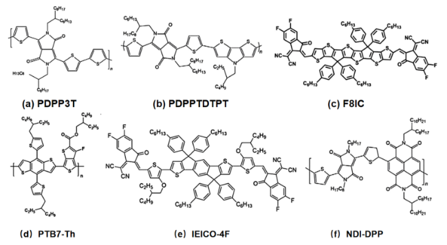
图8 采用(a) PDPP3T[88];(b) PDPPTDTPT[89]; (c) F8IC[94]; (d) PTB7-Th[92]; (e) IEICO-4F[92]; (f) NDI-DPP[93]有机材料与钙钛矿复合,拓宽钙钛矿PDs的光谱响应范围Fig.8 The structural formula of (a) PDPP3T[88]; (b) PDPPTDTPT[89]; (c) F8IC[94]; (d) PTB7-Th[92]; (e) IEICO-4F[92]; (f) NDI-DPP[93]; which are adopted to combine with perovskite to broaden the spectral response range of Pb perovskite-based PDs. |
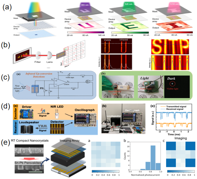
图10 (a) 用于图像传感的PbS-SCN/MAPbI3 PDs阵列的设计和演示图[81] ;(b) OIHP PDs的图像扫描系统示意图和实际成像图[99] ;(c) 近红外上转换检测系统示意图[41] ;(d) 光电探测器集成近红外声光通信系统示意图[46] ;(e) 6×6像素Sn/Pb钙钛矿器件的光电流分布和捕获图像[39]Fig10 (a) Design and demonstration of a PbS-SCN/MAPbI3 photodetector array for image-sensing application[81] ;(b) Schematic of the image scanning system and actual imaging for the OIHP photodetector[99] ;(c) Schematic diagram of the NIR up-conversion detection system with pictures of experimental detection under weak light and darkness to avoid the effects of indoor lighting[41] ;(d) Schematic diagram of the integrated NIR acousto-optic communication system with mixed perovskite photodetector[46] ;(e) Photocurrent distribution and capture images of 6 × 6 pixel Sn/Pb chalcogenide devices[39] Copyright 2019,American Chemical Society. Copyright 2020, Nature. Copyright 2020, Wiley-VCH. Copyright 2021,Elsevier. Copyright 2021, American Chemical Society. |
| [1] |
|
| [2] |
|
| [3] |
|
| [4] |
|
| [5] |
|
| [6] |
|
| [7] |
|
| [8] |
|
| [9] |
|
| [10] |
|
| [11] |
National Renewable Energy Laboratory, (2023). https://www.nrel.gov/pv/interactive-cell-efficiency.html.
|
| [12] |
|
| [13] |
|
| [14] |
|
| [15] |
|
| [16] |
|
| [17] |
|
| [18] |
|
| [19] |
|
| [20] |
|
| [21] |
|
| [22] |
|
| [23] |
|
| [24] |
|
| [25] |
|
| [26] |
|
| [27] |
|
| [28] |
|
| [29] |
|
| [30] |
|
| [31] |
|
| [32] |
|
| [33] |
|
| [34] |
|
| [35] |
|
| [36] |
|
| [37] |
|
| [38] |
|
| [39] |
|
| [40] |
|
| [41] |
|
| [42] |
|
| [43] |
|
| [44] |
|
| [45] |
|
| [46] |
|
| [47] |
|
| [48] |
|
| [49] |
|
| [50] |
|
| [51] |
|
| [52] |
|
| [53] |
|
| [54] |
|
| [55] |
|
| [56] |
|
| [57] |
|
| [58] |
|
| [59] |
|
| [60] |
|
| [61] |
|
| [62] |
|
| [63] |
|
| [64] |
|
| [65] |
|
| [66] |
|
| [67] |
|
| [68] |
|
| [69] |
|
| [70] |
|
| [71] |
|
| [72] |
|
| [73] |
|
| [74] |
|
| [75] |
|
| [76] |
|
| [77] |
|
| [78] |
|
| [79] |
|
| [80] |
|
| [81] |
|
| [82] |
|
| [83] |
|
| [84] |
|
| [85] |
|
| [86] |
|
| [87] |
|
| [88] |
|
| [89] |
|
| [90] |
|
| [91] |
|
| [92] |
|
| [93] |
|
| [94] |
|
| [95] |
|
| [96] |
|
| [97] |
|
| [98] |
|
| [99] |
|
/
| 〈 |
|
〉 |