Home Journals Progress in Chemistry
Progress in Chemistry

Abbreviation (ISO4): Prog Chem      Editor in chief: Jincai ZHAO

About  /  Aim & scope  /  Editorial board  /  Indexed  /  Contact  / 
12

Recent Advances in Quasi-Two-Dimensional Blue Perovskite Light- Emitting Diodes

  • Juan Ma 1 ,
  • Ruiyu Yang 1 ,
  • Yanfeng Chen 1, 2 ,
  • Ying Liu 1 ,
  • Shufen Chen , 1, 2, *
Expand
  • 1 School of Materials Science and Engineering, Nanjing University of Posts and Telecommunications, Nanjing 210023, China
  • 2 State Key Laboratory of Organic Electronics and Information Displays, Nanjing University of Posts and Telecommunications, Nanjing 210023, China
* Corresponding author e-mail:

Received date: 2023-07-10

  Revised date: 2023-10-27

  Online published: 2023-12-29

Supported by

National Natural Science Foundation of China(62074083)

Science and Technology Project of Jiangsu (Science and Technology Cooperation Project of Hong Kong, Macao and Taiwan(BZ2023059)

Natural Science Fund for Colleges and Universities in Jiangsu Province(20KJA510005)

Project of State Key Laboratory of Organic Electronics and Information Displays(GDX2022010009)

Postgraduate Research & Practice Innovation Program of Jiangsu Province(KYCX21_0781)

Abstract

Blue perovskite light-emitting diodes (PeLEDs) restrict the rapid development of full-color display and white lighting technology of perovskite. Quasi-two-dimensional (Q2D) perovskite enables to realize blue light emission via strict control on layer number and use of quantum confinement effect and can significantly improve the stability of perovskite film and PeLEDs by using hydrophobic organic ligands, which has gradually become a research hotspot in the field of perovskites. This review summarizes the research progress on Q2D blue PeLEDs from three aspects of component engineering, film process and device optimization, and analyzes the challenges faced by Q2D blue PeLEDs and the efficiency improvement approaches. At last, this paper envisages the future research direction and feasible solutions.

Contents

1 Introduction

2 Overview of quasi-two-dimensional perovskites

3 Research progress of quasi-two-dimensional blue perovskite light-emitting diodes

3.1 Component engineering

3.2 Film process optimization

3.3 Device structure optimization

4 Challenges faced by quasi-two-dimensional blue light-emitting perovskites

4.1 Photoluminescence quantum efficiency

4.2 Spectral stability

4.3 Phase purity

4.4 Charge injection efficiency and interface engineering

5 Conclusion and outlook

Cite this article

Juan Ma , Ruiyu Yang , Yanfeng Chen , Ying Liu , Shufen Chen . Recent Advances in Quasi-Two-Dimensional Blue Perovskite Light- Emitting Diodes[J]. Progress in Chemistry, 2024 , 36(2) : 224 -233 . DOI: 10.7536/PC230705

1 Introduction

Metal halide perovskite generally refers to materials with the general chemical formula of Metal halide perovskite, which is named after Russian geologist Lev Perovski, in which the A-site is usually methylamine ion (MA+.CH3NH3+), formamidinium ion (FA+, CH3CH2NH3+), cesium ion (Cs+), etc.The B site is a divalent metal cation such as Pb2+, Sn2+ and the like,The X position is I-, Br, U Cl halide anion or their mixture, as shown in Fig. 1[1]. Perovskites have excellent optoelectronic properties, including large absorption coefficient, high fluorescence quantum yield (PLQY), high carrier mobility, and long diffusion length[2]. Compared with organic light-emitting devices (OLEDs), perovskite light-emitting devices (PeLEDs) have the characteristics of narrow half-peak width, high color purity and wide color gamut, so PeLEDs are ideal light-emitting devices[3].
图1 钙钛矿的晶体结构示意图

Fig. 1 Crystal structure of perovskites

Since Friend et al. First observed the electroluminescence phenomenon of three-dimensional perovskite PeLEDs at room temperature in 2014, the field of PeLEDs has experienced rapid development, in which the External quantum efficiency (EQE) of green, red and near-infrared PeLEDs has now exceeded 22%[4][5~7]. In 2023, Xuan's team used Ni0.9Mg0.1Ox film with high refractive index and high hole mobility as the hole injection layer to balance the injection of charge carriers, and its device achieved an external quantum efficiency of 30.84% at a brightness of 6514 cd/m2, setting the latest world record for the efficiency of green PeLEDs[5]. As an important part of display and lighting, the performance of blue PeLEDs is far behind that of PeLEDs with other light colors, which is due to a series of problems such as low PLQY, poor film quality, unbalanced electron-hole injection, deep valence band energy and poor spectral stability.
At present, there are three ways to achieve blue light emission of perovskite, including composition control, dimension control and size control[8,9]. In order to achieve blue emission, the following methods can be used to widen the band gap of perovskite. The most common method is to adjust the composition of perovskite, such as adjusting the Cl/Br ratio in CsPbX3, which can increase the band gap from 2. 4 eV to 3. 0 eV, thus achieving the transition from green to blue light[10]. However, the mixed halide perovskite thin films prepared based on this method have poor quality and low PLQY, which are prone to ion migration, resulting in phase separation and the appearance of green light. In addition, the formation of low-dimensional phase perovskite can also be induced by introducing bulky A-site cations to replace the small-sized cations in the perovskite precursor. When low dielectric constant cations are intercalated into perovskite to form quantum well structure, quantum confinement effect and energy funneling effect will occur, which will lead to blue shift of spectrum and blue emission[11]. Up to now, the highest reported EQE of sky blue PeLEDs is 18.65%, which is the efficiency record set by Tang Jianxin's team at Soochow University[12]; Deep blue PeLEDs are inefficient and difficult to implement, so the highest EQE so far is only 5.5%[13]. From the existing results, there is still a big gap between the performance of blue PeLEDs and their commercial applications, and besides efficiency, device lifetime is also the biggest bottleneck hindering their commercialization[14,15]. In recent years, Quasi-two-dimensional perovskite (Q2DPe) has been widely concerned and reported, which can significantly improve the stability of films and devices while maintaining high efficiency, and is considered to be the best solution to the related challenges of efficiency and stability of blue LEDs so far.

2 Overview of quasi-two-dimensional perovskites.

Unlike 3D perovskites, which have homogeneous compositions, quasi-2D perovskite films are mixtures composed of 2D perovskites with different quantum well structures, i.e., different n values (n ≥ 1, an integer). Two-dimensional perovskite materials are those in which perovskite crystal growth is not restricted in two dimensions and is restricted to the nanoscale range in the third dimension[16]. In crystallography, two-dimensional perovskites are obtained by cutting along the three-dimensional perovskite structure, thus forming < 100 >, < 110 >, and < 111 > -oriented 2D perovskites, respectively. Among them, < 100 > -oriented 2D perovskites are the most prevalent, which are divided into Ruddlesden-Popper (RP) phase containing two monoamines, Dion-Jacobson (DJ) phase containing one diamine, and alternating cations in the interlayer (ACI) phase containing one guanidinium group, as shown in Figure 2[17]. The first blue PeLEDs based on RP-phase 2D perovskite, with phenylethylamine as the (PEA)2PbBr4(PEA, can separate the three-dimensional perovskite into layered two-dimensional perovskite due to the large ionic radius of the PEA+, and its emission peak is 410 nm at room temperature, but the EQE is only 0.04%[17]; While the first blue PeLEDs based on DJ-phase quasi-2D perovskite was realized by introducing the aromatic polyamine molecule 1,4-xylylenediamine bromide (P-PDABr2) into the perovskite precursor solution, and its maximum brightness can reach 211 cd·m−2 with the emission peak at 465 nm and the maximum EQE of 2.6%[19]. In addition, the chemical formulas of RP and DJ phase perovskites are L2An−1BnX3n+1 and LAn−1BnX3n+1, respectively, where L is an organic spacer cation (such as butylamine (BA), phenylethylamine (PEA), and 1,4-diaminobutane (DAB)),A represents a positive monovalent cation (Cs+, MA+, FA+, etc.),B represents a positive divalent metal cation (Pb2+, Mn2+, Cd2+, etc.), X is a halide anion or a mixture thereof, and n represents the number of layers of inorganic octahedra in the perovskite. When the organic cation in the A-site is large enough to maintain a stable bulk perovskite structure, the perovskite lattice will form a quasi-two-dimensional layered structure. In addition to controlling the number of layers to achieve blue emission, the blue emission can also be achieved by changing the ratio of Cl/Br in the X site. However, the introduction of chloride ions can increase the density of defect States and induce phase separation. Therefore, in order to achieve efficient and stable blue PeLEDs, it is essential to introduce appropriate passivators to reduce the defect state density of perovskite films and inhibit the internal halide ion migration. Tang Jianxin's team successfully prepared efficient sky-blue perovskite LEDs with stable spectral emission by controlling ionic behavior with bifunctional additives, that is, using passivation salts composed of Lewis benzoate anions and alkali metal cations as passivators, while passivating uncoordinated lead ions and inhibiting the migration of halide ions[12]. The device has a luminescence peak at 483 nm and a maximum EQE of 18.65%, which is the highest efficiency of quasi-two-dimensional blue perovskite LEDs reported so far.
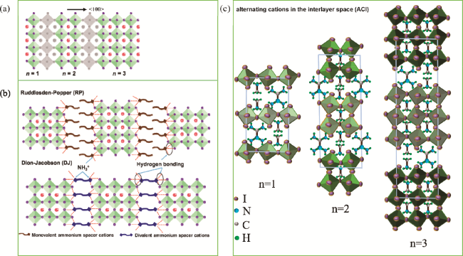
图2 (a) 间隔阳离子从<100>晶面将三维钙钛矿切割成层状钙钛矿的结构示意图[17];(b) RP和DJ相层状钙钛矿的晶体结构(n = 3)[17];(c) ACI相层状钙钛矿的晶体结构(n = 1,2,3)

Fig. 2 (a) Structure derivation of a layered perovskite with spacer cations cutting the 3D perovskite from the <100> plane[17], Copyright 2019, American Chemical Society; (b) crystal structures of RP and DJ phase layered perovskites (n = 3)[17], Copyright 2019, American Chemical Society; (c) crystal structures of layered perovskite of ACI phase (n = 1, 2, 3).

Quasi-two-dimensional perovskite materials usually contain a variety of perovskite nanosheets with different layers (such as n = 1, 2, 3, etc.) And some three-dimensional perovskites, so they often have multiple photoluminescence peaks and wide half-peak widths, as shown in Figure 3A[20]. Compared with 3D perovskites, the band gap of quasi-2D perovskites gradually increases with the decrease of the number of layers, as shown in Fig. 3B.
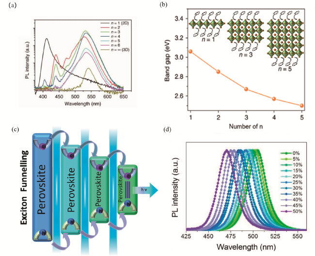
图3 (a) 不同n值的PEA2(FAPbBr3)n−1PbBr4的PL光谱[22];(b) Q2DPe的带隙,插图是n=1,3,5的准2D的钙钛矿的原子模型[23];(c) 小n相Q2DPe到大n相Q2DPe之间电荷转移或激子漏斗的能带图;(d) 不同氯化物含量的一系列准二维PBABr:CsPbBrxCl3−x 钙钛矿薄膜的归一化PL光谱[24]

Fig. 3 (a) PL spectra of PEA2(FAPbBr3)n−1PbBr4 with different n values[22], Copyright 2018, Nature Publishing Group; (b) band gaps of quasi-2D perovskites, illustrated as atomic models of quasi-2D perovskites with n=1, 3, and 5[23], Copyright 2019, Wiley-Blackwell; (c) energy band diagram of charge transfer or funneling of excitons between Q2DPe of small n to large n phase; (d) normalized PL spectra for a series of quasi-2D PBABr:CsPbBrxCl3−x perovskite films with different chloride content[24], Copyright 2019, American Chemical Society.

Because the band gaps of perovskites with different dimensions and different layers are also different, a natural energy funnel structure can be formed, and the energy is gradually transferred from the two-dimensional perovskite with smaller n to the two-dimensional perovskite with larger n, as shown in fig. 3C[20]. The energy transfer efficiency is also one of the important factors affecting the device performance, which is related to the absorption spectrum overlap between the donor (perovskite with smaller layer number) PL and the acceptor (perovskite with larger layer number), the distance between the acceptor and the donor, and the acceptor concentration[21]. In addition, the strong quantum confinement effect in quasi-two-dimensional perovskite materials can significantly shift the photoluminescence and Electroluminescence (EL) peaks to blue compared with three-dimensional perovskite. By changing the number of [PbBr6]4− octahedral layers and the proportion of halogens, the EL peak position of quasi-two-dimensional perovskite materials can also be changed, as shown in Figure 3A, d.

3 Research Progress of Quasi-two-dimensional Blue Light Perovskite

3.1 Component engineering

The introduction of bulky amine salts into perovskite can inhibit the growth of perovskite in one direction, while replacing part of the small A-site cations in perovskite, inducing the formation of quasi-two-dimensional perovskite[23]. These amine salts can not enter the lattice because of their large size, and generally appear on the surface of quasi-two-dimensional perovskite, which can passivate the charged defects on the surface of perovskite, thus reducing non-radiative recombination and making perovskite show excellent optical properties; In addition, charge carriers are confined in an inorganic octahedral structure by the amine salt, and the perovskite has a quantum well structure due to the large difference in dielectric constants, so that a strong quantum confinement effect and a large exciton binding energy are exhibited, so that the emission wavelength is blue shifted, and the radiation emission performance is enhanced. Generally speaking, taking lead halide perovskite as an example, the band gap of perovskite is determined by the p orbital of halogen and the 6p orbital (conduction band) and 6s orbital (valence band) of Pb metal cation, respectively. In quasi-two-dimensional or two-dimensional perovskite,The emission wavelength of perovskite can be greatly controlled by changing the number of inorganic octahedral layers n and its strong quantum confinement effect, which is also a common means for researchers to prepare blue perovskite[25][26,27].
In addition to controlling the n value, selecting the appropriate A-site cation can also control the emission wavelength and improve the luminescence quantum yield (PLQY) of perovskite. Tisdale et al. Found that the PLQY of quasi-2D perovskite with MA+ as A-site cation was only 6%, but the PLQY of quasi-2D perovskite with FA+ as A-site cation could be improved to 22%[28]. The calculation results of Zhumekenov et al. Show that the formation energy of bromine vacancy and bromine interstitial defects in FAPbBr3 is higher than that in MAPbBr3, which makes the density of defect States in FAPbBr3 lower, so the PLQY can be significantly improved[29]. In addition, the formation of a quasi-two-dimensional perovskite structure is favored when the A-site cations in the outer layer are replaced by positive monovalent long alkyl chains such as octylamine (OCTA+), ethylamine (EA+), butylamine (BA+), and phenylethylamine (PEA+[23]. Chu et al. Introduced phenylethylamine ions into the quasi-two-dimensional perovskite PEA2(CsPbBr3)2PbBr4, and found that it could enter the perovskite lattice and partially replace the Cs+, thus changing the Pb-Br orbital coupling and increasing the band gap, realizing the regulation of the emission range of 466 – 508 nm, and the maximum EQE of the sky-blue device with an EL peak position of 488 nm could reach 12.1%, as shown in Fig. 4A and B[15].
图4 (a) PEA2(Cs1−xEAxPbBr3)2PbBr4钙钛矿LED的外量子效率(EQE)与电流密度的关系[15];(b) PEA2(Cs1−xEAxPbBr3)2PbBr4钙钛矿LED的归一化电致发光(EL)光谱[15];(c) CsPbBr3: PEACl:YCl3薄膜辐射复合示意图[30];(d) 不同YCl3含量PeLEDs的EQE曲线。插图为点亮的PeLEDs照片[30]

Fig. 4 (a) Characterization of external quantum efficiency (EQE) versus current density of PEA2(Cs1−xEAxPbBr3)2PbBr4 perovskite LED[15], Copyright 2020, Nature Publishing Group; (b) normalized electroluminescence (EL) spectra of PEA2(Cs1−xEAxPbBr3)2PbBr4 PeLED[15], Copyright 2020, Nature Publishing Group; (c) schematic illustration of the yttrium distribution and radiation recombination within the CsPbBr3:PEACl:YCl3 thin-film[30], Copyright 2019, Nature Publishing Group; (d) EQE curves of PeLEDs with different YCl3 percentages. Inset shows the digital photographic image of the operating PeLED[30], Copyright 2019, Nature Publishing Group.

In addition, the precise control of the ratio of the mixed halide (Cl/Br) can also realize the control of the luminescence peak and the absorption peak position of the quasi-two-dimensional perovskite material. Wang et al. Introduced phenylethylamine chloride (PEACl) and additive yttrium chloride (YCl3) into a three-dimensional CsPbClxBr3−x system to form a quasi-two-dimensional perovskite[30]. It is found that with the addition of YCl3, more yttrium ions (Y3+) are enriched on the surface or grain boundary of the film, resulting in the widening of the band gap of the film, which limits the carriers inside the perovskite grains, and then radiates recombination luminescence, as shown in Figure 4C. The maximum brightness of PeLEDs with 2%YCl3 content can be as high as 9040 cd·m−2, and the EL peak position is 485 nm, corresponding to an EQE as high as 11% (Figure 4D).
It should be noted that mixed-halogen quasi-2D perovskites may lead to the migration of halide ions under the action of external electric field, and then produce phase separation phenomenon. In addition, polar solvents, temperature, humidity, oxygen concentration and other external factors can also induce changes in the crystal structure, resulting in phase separation of perovskite, which eventually leads to spectral shift, color purity reduction, external quantum efficiency decline, and device stability deterioration.

3.2 Film Process Optimization

The perovskite nanosheets prepared based on the traditional LARP method are dispersed in poor solvents such as toluene, and the film prepared by spin coating has many holes, and there are a large number of grain boundaries between the nanosheets. A large number of defects make the electron transport layer directly contact with the hole injection layer, resulting in a large leakage current and a decline in device performance[31]. Nanocrystal pinning (NCP) is a film formation method in which a quasi-two-dimensional perovskite precursor is directly spin-coated on a substrate, and an anti-solvent toluene is added dropwise during spin-coating to induce perovskite crystallization (Figure 5A)[32]. According to Lee et al., during the crystallization of RP-phase quasi-two-dimensional perovskite, toluene antisolvent can instantaneously replace DMSO/DMF molecules originally adsorbed on the (001) crystal plane, which to some extent eliminates the oriented in-plane growth of quasi-two-dimensional perovskite grains and promotes their random orientation growth[33]. They believe that this structure-modulated nanocrystal can improve the charge transport ability by increasing the contact surface. Butylammonium bromide (BABr) is an organic macromolecule with poor conductivity. Wang et al. Used isopropanol as a cleaning agent to remove part of BABr, and successfully increased the EQE of perovskite LEDs from 1.81% to 8.42%[34].
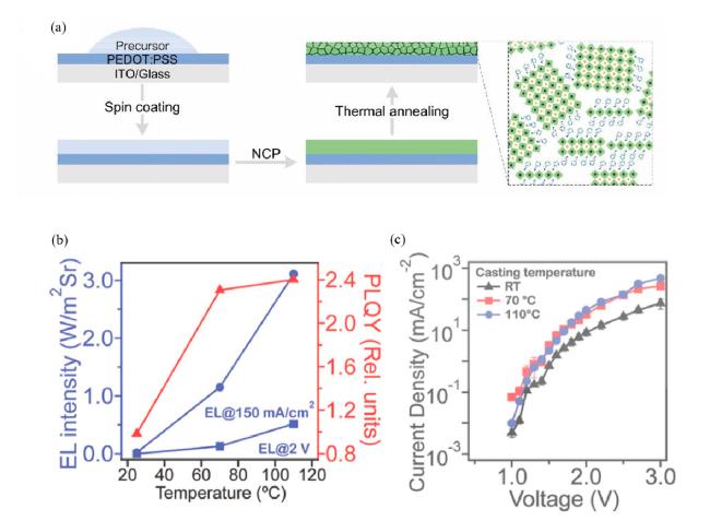
图5 (a) NCP法制备准二维钙钛矿膜层示意图[32];(b) 固定电流密度和电压下(BA)2(MA)2Pb4I13的EL强度和PLQY[36];(c) 不同温度下(BA)2(MA)2Pb4I13的J-V特性曲线[36]

Fig. 5 (a) Schematic diagram of quasi-two-dimensional perovskite film prepared by NCP method[32], Copyright 2019, Royal Society of Chemistry; (b) EL intensity as a function of casting temperature at a fixed current density and fixed voltage and PLQY as a function of casting temperature for (BA)2(MA)2Pb4I13(Pb4) LEDs[36], Copyright 2018, Wiley-Blackwell; (c) J-V characteristic curves for LEDs using (BA)2(MA)2Pb4I13 casted by different temperatures[36], Copyright 2018, Wiley-Blackwell.

Doping appropriate amount of additives into the perovskite precursor can effectively reduce the film defects and improve the quality of perovskite films. Ma et al. Doped Poly ethylene oxide (PEO) into quasi-two-dimensional perovskite Poly ethylene oxide and successfully prepared PEO-CsPbI3 mixed film[35]. PEO passivates the defects on the perovskite surface without changing the emission peak position, which improves its PLQY, and the brightness of the device reaches 1392 cd·m−2, and the maximum EQE can reach 6.23%. However, when the film was prepared by direct spin-coating of perovskite precursor solution, the monolayer and bilayer nanosheets grew parallel to the substrate, which seriously hindered the charge transport in the vertical direction. To this end, Mohite et al. Realized a vertically oriented quasi-two-dimensional perovskite by thermal spin-coating treatment, thus effectively promoting the injection and transport of carriers[36]. Meanwhile, the developed thermal spin coating method was applied to deposit RP perovskite thin films, proving that the annealing temperature is the key factor to achieve the preferred orientation of perovskite grains. In addition, the surface energy of the substrate promotes the ordered growth of the inorganic lamellar structure of layered perovskite along the out-of-plane, further achieving efficient charge transport. Compared with the pure 2D device processed at low temperature, the device with thermal spin coating exhibits a higher current density, its EL intensity shows a 1500-fold boost, and its PLQY is about 2.4%, which is about 2.5 times that of the room-temperature processed film (Fig. 6 B, C).
图6 (a) 电流密度和亮度随电压变化的特征曲线[37];(b) EQE与电流密度的关系[37];(c) 混合卤化物钙钛矿的相分离[11]; (d) 准二维PeLEDs的三明治夹层结构

Fig. 6 (a) Current-voltage-luminance characteristic curves[37], Copyright 2020, Nature Publishing Group; (b) characterization of EQE versus current density[37], Copyright 2020, Nature Publishing Group; (c) phase segregation of mixed-halide perovskites [11], Copyright 2022, Nature Publishing Group; (d) the sandwich-like interlayer structure of quasi-2D PeLEDs

表1 蓝色和天蓝色Q2D PeLEDs的性能参数总结

Table 1 Summary of performance parameters of blue and sky-blue Q2D PeLEDs

Perovskite material Device structure EL Peak (nm) EQE (%) Vt/(V) Ref
PEA2Cs1.6MA0.4Pb3Br10
treated with DPPOCl
ITO/PEDOT:PSS:PFI/Q2DPe/TPBi/LiF/Al 479 5.2 - 14
PEA2(Rb0.6Cs0.4)Pb3Br10 ITO/PEDOT:PSS/Q2DPe/TmPyPB/LiF/Al 475 1.35 3 15
(PEA)2PbBr4 ITO/PEDOT:PSS/2D perovskite/TPBi/Ca/Al 410 0.04 2.5 18
P-PDA,PEACsn−1PbnBr3n+1 ITO/PVK/PFI/Q2DPe/3TPYMB/Liq/Al 465 2.6 - 19
PEACl:CsPbBr3:YCl3 ITO/TB(MA)/Q2DPe/TPBi/LiF/Al 488 13.5% 6 38
CsPbBr3:PEACl:YCl3 ITO/PEDOT:PSS/PVK/Q2DPe/TPBi/LiF/Al 485 11 3 30
PEA2Csn−1Pbn(Br/Cl)3n+1 ITO/PEDOT:PSS/Q2DPe/TPBi/LiF/Al 480 5.7 3.2 37
(Cs/Rb/FA/PEA/K)Pb(Cl/Br)3 ITO/LiF/Q2DPe/LiF/Bphen/LiF/Al 484 2.01 -- 39
EA2(MA)n−1PbnBr3n+1 ITO/PEDOT:PSS/Q2DPe/TmPyPB/CsF/Al 485 2.6 3.4 42
OLA2MAn−1PbnBr3n+1 ITO/PEDOT:PSS/PVK/Q2DPe/TPBi/LiF/Al 456 0.0046 3.4 43
BA2MA2Pb3Br7Cl3 ITO/PEDOT:PSS/Poly-TPD /Q2DPe/TPBi/LiF/Al 468 0.01 5.2 44
POEA2MAn−1PbnBr3n+1 ITO/PEDOT:PSS/Q2DPe/TPBi/Ba/Al 480 1.1 3.6 45
BA2Csn−1Pbn(Br/Cl)3n+1 ITO/PEDOT:PSS/Q2DPe/TPBi/Al 487 6.2 4.5 46
PBA2Csn−1Pbn(Br/Cl)3n+1 ITO/NiOx/LiF/Q2DPe/TPBi/LiF//Al 490 0.52 - 24
(IPA:PEA)2(MA:Cs)n−1Pbn
Br3n+1
ITO/PEDOT:PSS/Q2DPe/TPBi/LiF/Al 490 1.9 5 47
BA2DMA1.6Cs2Pb3Br11.6 ITO/PEDOT:PSS or NiOx/Q2DPe/TPBi/LiF/Al 490 2.4 3.3 48
PEA2DMA1.2Cs2Pb3Br11.2 ITO/PEDOT:PSS or NiOx/Q2DPe/TPBi/LiF/Al 499 1.58 4.4 48
(PEA:NPA)Csn−1PbnBr3n+1 ITO/poly(N-vinylcarbazole)/PVK/Q2DPe/
PO-T2T/Liq/Al
485 2.62 2.6 49
(PBABr):(Cs/FA/MA)Br:PbBr2 ITO/PEDOT: PSS/Q2DPe/PO-T2T/LiF/Al 465 2.34 2.8 50
PBA2(FACs)n−1PbnBr3n+1 ITO/NiOx/TFB/PVK/Q2DPe/TPBi/LiF/Al 483 9.5 3.3 51

3.3 Device structure optimization

Quasi-two-dimensional PeLEDs usually adopt a sandwich structure, that is, a hole injection or transport layer, a perovskite light-emitting layer, and an electron transport or injection layer are prepared between a transparent anode (generally ITO) and a metal cathode (Ag, Al, etc.). After a bias voltage is applied to the PeLEDs, holes are injected from one side of the ITO anode and conducted to the perovskite layer through the hole injection layer and the hole transport layer; The electrons are injected from the side of the metal cathode and conducted to the perovskite layer through the electron injection layer and the electron transport layer, and finally, the electrons and the holes are radiated and recombined in the perovskite layer to emit light. Common hole transport/injection materials include poly (3,4-ethylenedioxythiophene) -polystyrenesulfonic acid (PEDOT: PSS), di (naphthalen-1-yl) -N, N ′ -di (phenyl) benzidine (NPB), N, N ′ -bis (3-methylphenyl) -N, N-diphenyl-1,1 ′ -biphenyl-4,4 ′ -diamine (TPD), etc; Common electron transport/injection materials are 1,3,5-tris (1-phenyl-1H-benzimidazol-2-yl) benzene (TPBi), 3,3 ′- [5 ′- [3- (3-pyridyl) phenyl] (TmPyPb), 4,6-bis (3,5-di (3-pyridyl) phenyl) -2-methylpyrimidine (B3PYMPM), etc. The thickness of the transport or injection layer will affect the number of carriers injected into the light-emitting layer, and also determine the recombination region and recombination rate of carriers, so the optimization of the thickness of the carrier transport layer will affect the performance of PeLEDs.
Li et al. Observed the effect of the thickness of PEDOT: PSS (15 ~ 60 nm) on the luminescent performance of the device, and found that when the thickness of PEDOT: PSS is thicker (60 nm), the time for the injected holes to pass through the PEDOTPSS film is prolonged, and when the injected holes are injected into the valence band of perovskite, the recombination region is closer to the B region[37]; However, when the thickness of PEDOT: PSS is thin (15 nm), the PEDOT: PSS film can not cover the ITO well, resulting in a large leakage current when the perovskite crystal is directly contacted with the electrode. Therefore, when the thickness of PEDOT: PSS is optimized to 30 nm, the position of the recombination region is moved to the A region, and the leakage current is reduced. By modulating the recombination region, the turn-on voltage can be reduced to 3.2 V, blue emission with EL peak at 480 nm is achieved, and the maximum brightness of the device can reach 3780 cd/m2 with an EQE of 5.7%, as shown in Figure 6A, B.
Interface engineering is also an important way to improve the efficiency and structural stability of perovskite devices. For example, PEDOT: PSS is an acidic material, which will corrode the ITO electrode and perovskite active layer, resulting in poor efficiency and stability of perovskite LEDs. In response to the above problems, Xu Baomin's team synthesized a new neutral polyelectrolyte material TB (MA) as a hole transport layer[38]. The neutral TB (MA) material does not corrode the electrode, and its hydrophilic property contributes to the denser and more uniform growth of the quasi-two-dimensional perovskite film. Compared with the traditional acidic PEDOT: PSS, the EQE of the quasi-two-dimensional blue PeLEDs prepared by the material is increased from 7. 8% to 13. 5%, and the working stability of the device is significantly improved, and the T50 lifetime of the device can reach 290 at a constant voltage of 5 V, which is 2. 3 times longer than that of the light-emitting device based on PEDOT: PSS.
In addition, it should be noted that due to the deep valence band of blue perovskite, there are charge injection imbalance, carrier accumulation and interface recombination problems at the perovskite/HTL interface[39]. In order to effectively improve the charge injection efficiency and radiation recombination of the perovskite film, a lithium fluoride (LiF) layer with a controllable thickness is used at the Q2DPe interface to induce and balance the charge injection.The LiF layer at the ITO/Q2DPe interface suppresses fluorescence quenching by reducing the injection barrier and interfacial recombination, and the maximum EQE of the obtained device can reach 2. 01%, and the lifetime of the device after interface modification (300 min) is longer than that of the control device (20 min)[39]. On the one hand, the improvement of device stability depends on the uniform perovskite film with high quality, and on the other hand, it is also closely related to the suppression of ion migration by the LiF layer at the Q2DPe interface[39].

4 Challenges for quasi-two-dimensional blue light perovskites

4.1 Photoluminescence quantum efficiency

The PLQY of wide band gap blue perovskite films is generally low, which is due to the fact that the recombination center formed by the deep level defects of blue perovskite increases the non-radiative recombination channel, thus leading to the decrease of PLQY; Secondly, due to the partial radiative recombination of defect levels, the emission spectrum may be red-shifted or multi-peak emission, resulting in low color purity. In addition, the shedding of organic ligands during spin coating can induce the agglomeration of perovskite grains, which in turn leads to the fluorescence quenching and the decrease of PLQY. However, low PLQY is not conducive to the improvement of device performance, so it is very important to improve the PLQY of perovskite thin films for the development of efficient quasi-two-dimensional blue PeLEDs.

4.2 Stability

In the mixed halide perovskite thin film, external factors such as light, heat, and humidity can lead to phase separation, as shown in Figure 6C. At the same time, excitons will migrate from the perovskite phase dominated by Cl to the perovskite phase dominated by Br. Due to the lattice mismatch, unstable local areas will be produced at the interface between the two phases, which will lead to the decomposition of perovskite. With the migration of halogen ions, red shift of the spectrum can be observed, which is not conducive to blue emission[11]. Phase separation can be effectively avoided by using single halide perovskite, but the introduction of spacer cations in low-dimensional perovskite and perovskite nanocrystals is the main reason for the instability of blue perovskite films. The weak interaction between the organic spacer cations may reduce the stability of the quasi-2D perovskite[40].
In order to solve the stability problem of single halide perovskites, it is necessary to solve the unstable factors caused by organic spacers and surface ligands, that is, the weak interaction caused by van der Waals gap. The diammine end group of DJ phase perovskite can form hydrogen bonds with perovskite crystals on both sides, and can reduce the gap between crystal layers by reducing the chain length of spacer molecules, so as to increase the van der Waals force between molecules, thus achieving a stable perovskite film. An asymmetric spacer material called N, N-dimethyl-1,3-propanediamine (DPDA) was proved to be effective in maintaining the phase stability of DJ phase perovskite, which is better than that of the symmetric structure[40]. At the same time, ammonium ions with functional terminal groups can also meet the requirement of reducing the van der Waals gap in quasi-two-dimensional perovskites.

4.3 Phase purity

In quasi-two-dimensional perovskites, the distribution of mixed phases has a significant impact on the luminescence efficiency, charge transport and phase stability of the films. Q2DPe has many n = 1 phases, which is one of the main reasons for the poor charge transport performance. Reducing the formation of n = 1 phases directly by reducing the proportion of long-chain cations will produce too many three-dimensional phases (n = ∞), resulting in a red shift in the spectrum. Therefore, reducing the number of low-n phases and not introducing too many three-dimensional phases are the key to obtain high-performance blue quasi-two-dimensional perovskites by changing the type of long-chain cations or introducing binary, ternary ligands and diamine ligands.The phase distribution of the quasi-two-dimensional perovskite can be regulated and controlled, and the acting force between the organic layer and the inorganic layer can be improved, so that the perovskite light-emitting layer with high quantum yield, high stability and good transmission performance can be obtained. In addition to this, antisolvent rapid crystallization is also an effective strategy to obtain a more concentrated low-dimensional phase distribution.

4.4 Charge Injection Efficiency and Interface Engineering

Due to the deep valence band and low conduction band of blue perovskite, there is a large energy level difference between the perovskite layer and the charge transport layer, resulting in poor charge injection ability, a significant increase in the turn-on voltage of the device, and a significant decrease in efficiency. In addition, the high voltage and large electric field trigger the ion migration inside the perovskite, which further leads to the rapid degradation of the performance of blue PeLEDs. The introduction of transport materials matching the energy levels of the perovskite layer and the charge transport layer can reduce the carrier injection barrier and improve the luminescent performance and stability of the device. In addition, the modification of the buried interface or the upper surface of the perovskite by using Lewis acids and bases or zwitterions can effectively passivate defects, inhibit ion migration, and significantly reduce the corrosion of the perovskite by acidic transport layers (such as PEDOT: PSS), thereby improving the stability of the film and the device.

5 Conclusion and prospect

In this paper, the research progress of quasi-two-dimensional blue PeLEDs is summarized from three aspects of composition engineering, film optimization and device structure optimization, and the challenges of quasi-two-dimensional blue PeLEDs are analyzed, such as low photoluminescence quantum efficiency, poor stability and low charge injection efficiency.Although quasi-two-dimensional perovskite materials have been fully developed in recent years, there are still many problems in blue quasi-two-dimensional perovskite due to its late start. It is not ideal to use quasi-two-dimensional perovskite to achieve deep blue emission, its phase purity is low, and multi-phase emission will induce broad spectrum; The problem of low luminous efficiency can be improved by designing high PLQY, optimizing device structure and passivating film; By selecting a material system with a stable crystal structure, inhibiting the migration of halogen ions, and constructing an efficient and reasonable device structure, the stability of the device is improved.
Generally speaking, the quasi-two-dimensional perovskite grows parallel to the substrate, and carriers are transported laterally in it. For light-emitting devices where carriers need to be transported perpendicular to the substrate, the quasi-two-dimensional perovskite parallel to the substrate is not conducive to the injection and transport of carriers.Therefore, in order to improve the device luminescence efficiency, it is necessary to adjust the growth of quasi-2D perovskite to vertical orientation, such as selecting the appropriate annealing temperature and using DMF: DMSO mixed solvent system.
In addition, the ligands used in traditional RP-type quasi-2D perovskites are all single NH3+structure with large intergrain distance and van der Waals band gap. However, DJ-type quasi-two-dimensional perovskites use ligands with NH3+ at both ends, which can connect with the [PbBr6]4− layer at both ends, showing a larger dissociation energy, so that two grains can be closely connected together, thus reducing the grain spacing, inhibiting the quantum effect, and ultimately promoting the transfer of carriers between layered perovskites. At present, DJ-type quasi-two-dimensional perovskites have been widely used in perovskite solar cells. Selecting conjugated building blocks and organic cations with short chain length (~ 44Å) and determining the position of NH3+ on the conjugated building blocks are expected to improve the charge transport ability of quasi-two-dimensional perovskites and reduce the structural distortion, which provides a feasible design scheme for improving the efficiency of quasi-two-dimensional PeLEDs.
At present, although quasi-two-dimensional perovskite materials have attracted wide attention in lighting, photovoltaic, display and other fields, stable quasi-two-dimensional perovskite materials need to be developed urgently in terms of long-term stability of devices and materials, which is of great significance for perovskite materials to enter industrial production and practical application. This paper summarizes the current research challenges and opportunities of quasi-two-dimensional blue PeLEDs, as well as the future research directions and feasible schemes based on quasi-two-dimensional blue PeLEDs. Researchers should devote more energy to the study of long-term stability in order to promote the commercialization and application of this material with excellent photoelectric properties.
[1]
Dou L T, Wong A B, Yu Y, Lai M L, Kornienko N, Eaton S W, Fu A, Bischak C G, Ma J, Ding T N, Ginsberg N S, Wang L W, Alivisatos A P, Yang P D. Science, 2015, 349: 1518.

[2]
Dong R, Fang Y, Chae J, Dai J, Xiao Z, Dong Q, Yuan Y, Centrone A, Zeng X C, Huang J. Adv. Mater., 2015, 27: 1912.

[3]
Zhang X, Lai Z, Tan C, Zhang H. Angew. Chem. Int. Ed., 2016, 55: 8816.

[4]
Tan Z-K, Moghaddam R S, Lai M L, Docampo P, Higler R, Deschler F, Price M, Sadhanala A, Pazos L M, Credgington D, Hanusch F, Bein T, Snaith H J, Friend R H. Nat. Nanotechnol., 2014, 9: 687.

[5]
Bai W, Xuan T, Zhao H, Dong H, Cheng X, Wang L, Xie R. J. Adv. Mater., 2023, 35: 2302283.

[6]
Jiang J, Chu Z, Yin Z, Li J, Yang Y, Chen J, Wu J, You J, Zhang X. Adv. Mater., 2022, 34: 2204460.

[7]
Sun Y, Ge L, Dai L, Cho C, Ferrer Orri J, Ji K, Zelewski S J, Liu Y, Mirabelli A J, Zhang Y, Huang J Y, Wang Y, Gong K, Lai M C, Zhang L, Yang D, Lin J, Tennyson E M, Ducati C, Stranks S D, Cui L S Greenham N C. Nature, 2023, 615: 830.

[8]
Zhou B, Qi Z, Dai M, Xing C, Yan D. Angew. Chem. Int. Ed., 2023, 62: e202309913.

[9]
Gao R., Yan D. Sci. Bull., 2023, 68: 770.

[10]
Protesescu L., Yakunin S., Bodnarchuk M I, Krieg F, Caputo R, Hendon C H, Yang R X, Walsh A, Kovalenko M V. Nano Lett., 2015, 15: 3692.

[11]
Yang X, Ma L, Yu M, Chen H-H, Ji Y, Hu A, Zhong Q, Jia X, Wang Y, Zhang Y, Zhu R, Wang X, Lu C. Light Sci. Appl., 2023, 12: 177.

[12]
Shen Y, Li Y Q, Zhang K, Zhang L J, Xie F M, Chen L, Cai X Y, Lu Y, Ren H, Gao X, Xie H, Mao H, Kera S, Tang J X. Adv. Funct. Mater. 2022, 32: 2206574.

[13]
Karlsson M, Yi Z, Reichert S, Luo X, Lin W, Zhang Z, Bao C, Zhang R, Bai S, Zheng G, Teng P, Duan L, Lu Y, Zheng K, Pullerits T, Deibel C, Xu W, Friend R, Gao F. Nat. Commun., 2021, 12: 361.

[14]
Ma D, Todorovic P, Meshkat S, Saidaminov M I, Wang Y K, Chen B, Li P, Scheffel B, Quintero-Bermudez R, Fan J Z, Dong Y, Sun B, Xu C, Zhou C, Hou Y, Li X, Kang Y, Voznyy O, Lu Z-H, Ban D, Sargent E H. J. Am. Chem. Soc., 2020, 142: 5126.

[15]
Chu Z, Zhao Y, Ma F, Zhang C X, Deng H, Gao F, Ye Q, Meng J, Yin Z, Zhang X, You J. Nat. Commun., 2020, 11: 4165.

[16]
Rao C N R, Gopalakrishnan K, Maitra U. ACS Appl. Mater. Interfaces, 2015, 7: 7809.

[17]
Huang P, Kazim S, Wang M, Ahmad S. ACS Energy Lett., 2019, 4: 2960.

[18]
Lee D E, Kim S Y, Jang H W. J. Korean Ceram. Soc., 2020, 57: 455.

[19]
Yuan S, Wang Z K, Xiao L X, Zhang C F, Yang S Y, Chen B B, Ge H T, Tian Q S, Jin Y, Liao L S. Adv. Mater., 2019, 31: 1904319.

[20]
Li M, Gao Q, Liu P, Liao Q, Zhang H, Yao J, Hu W, Wu Y, Fu H. Adv. Funct. Mater., 2018, 28: 1707006.

[21]
Hoffman J B, Alam R, Kamat P V. ACS Energy Lett., 2017, 2: 391.

[22]
Yang X, Zhang X, Deng J, Chu Z, Jiang Q, Meng J, Wang P, Zhang L, Yin Z, You J. Nat. Commun., 2018, 9: 1169.

[23]
Fang T, Zhang F, Yuan S, Zeng H, Song J. InfoMat, 2019, 1: 211.

[24]
Wang K H, Peng Y, Ge J, Jiang S, Zhu B S, Yao J, Yin Y C, Yang J N, Zhang Q, Yao H B. ACS Photonics, 2019, 6: 667.

[25]
Ravi VK, Markad GB, Nag A. ACS Energy Lett., 2016, 1: 665.

[26]
Dou L, Wong A B, Yu Y, Lai M, Kornienko N, Eaton S W, Fu A, Bischak C G, Ma J, Ding T, Ginsberg N S, Wang L W, Alivisatos A P, Yang P. Science, 2015, 349: 1518.

[27]
Akkerman Q A, Motti S G, Srimath Kandada A R, Mosconi E, D’Innocenzo V, Bertoni G, Marras S, Kamino B A, Miranda L, De Angelis F, Petrozza A, Prato M, Manna L. J. Am. Chem. Soc., 2016, 138: 1010.

[28]
Weidman M C, Seitz M, Stranks S D, Tisdale W A. ACS Nano, 2016, 10: 7830.

[29]
Zhumekenov A A, Saidaminov M I, Haque M A, Alarousu E, Sarmah S P, Murali B, Dursun L, Miao X H, Abdelhady A L, Wu T, Mohammed O F, Bakr O M. ACS Energy Lett., 2016, 1: 32.

[30]
Wang Q, Wang X, Yang Z, Zhou N, Deng Y, Zhao J, Xiao X, Rudd P, Moran A, Yan Y, Huang J. Nat. Commun., 2019, 10: 5633.

[31]
Chen S, Shi G. Adv. Mater., 2017, 29: 1605448.

[32]
Xia P, Lu Y, Yu H, Li Y, Zhu W, Xu X, Zhang W, Qian J, Shen W, Liu L, Deng L, Chen S. Nanoscale, 2019, 11: 20847.

[33]
Lee H D, Kim H, Cho H, Cha W, Hong Y, Kim Y H, Sadhanala A, Venugopalan V, Kim J S, Choi J W, Lee C L, Kim D, Yang H, Friend R H, Lee T W. Adv. Funct. Mater., 2019, 29: 1901225.

[34]
Wang Z, Wang F, Sun W, Ni R, Hu S, Liu J, Zhang B, Alsaed A, Hayat T, Tan Z a. Adv. Funct. Mater., 2018, 28: 1804187.

[35]
Tian Y, Zhou C, Worku M, Wang X, Ling Y, Gao H, Zhou Y, Miao Y, Guan J, Ma B. Adv. Mater., 2018, 30: 1707093.

[36]
Tsai H, Nie W, Blancon J C, Stoumpos C C, Soe C M M, Yoo J, Crochet J, Tretiak S, Even J, Sadhanala A, Azzellino G, Brenes R, Ajayan P M, Bulovic V, Stranks S D, Friend R H, Kanatzidis M G, Mohite A D. Adv. Mater., 2018, 30: 1704217.

[37]
Li Z, Chen Z, Yang Y, Xue Q, Yip H L, Cao Y. Nat. Commun., 2019, 10: 1027.

[38]
Liu Y, Zhang L, Chen S, Liu C, Li Y, Wu J, Wang D, Jiang Z, Li Y, Li Y, Wang X, Xu B. Small, 2021, 17: 2101477.

[39]
Yuan F, Ran C, Zhang L, Dong H, Jiao B, Hou X, Li J, Wu Z. ACS Energy Lett., 2020, 5: 1062.

[40]
Ahmad S, Fu P, Yu S, Yang Q, Liu X, Wang X, Wang X, Guo X, Li C. Adv. Mater., 2022, 34: 2205217.

[41]
Liu Y, Ono L K, Tong G, Bu T, Zhang H, Ding C, Zhang W. J. Am. Chem. Soc., 2021, 143: 19711.

[42]
Wang Q, Ren J, Peng X F, Ji X X, Yang X H. ACS Appl. Mater. Interfaces, 2017, 9: 29901.

[43]
Kumar S, Jagielski J, Yakunin S, Rice P, Chiu Y C, Wang M, Nedelcu G, Kim Y, Lin S, Santos E J G, Kovalenko M V, Shih C J. ACS Nano, 2016, 10: 9720.

[44]
Hu H, Salim T, Chen B, Lam Y M. Sci. Rep., 2016, 6: 33546.

[45]
Chen Z, Zhang C, Jiang X F, Liu M, Xia R, Shi T, Chen D, Xue Q, Zhao Y J, Su S, Yip H L, Cao Y. Adv. Mater., 2017, 29: 1603157.

[46]
Vashishtha P, Ng M, Shivarudraiah S B, Halpert J E. Chem. Mater., 2019, 31: 83.

[47]
Xing J, Zhao Y, Askerka M, Quan L N, Gong X, Zhao W, Zhao J, Tan H, Long G, Gao L, Yang Z, Voznyy O, Tang J, Lu Z H, Xiong Q, Sargent E H. Nat. Commun., 2018, 9: 3541.

[48]
Zeng S, Shi S, Wang S, Xiao Y. J. Mater. Chem. C, 2020, 8: 1319.

[49]
Jin Y, Wang Z K, Yuan S, Wang Q, Qin C, Wang K L, Dong C, Li M, Liu Y, Liao L S. Adv. Funct. Mater., 2020, 30: 1908339.

[50]
Yantara N, Jamaludin N F, Febriansyah B, Giovanni D, Bruno A, Soci C, Sum T C, Mhaisalkar S, Mathews N. ACS Energy Lett., 2020, 5: 1593.

[51]
Liu Y, Cui J, Du K, Tian H, He Z, Zhou Q, Yang Z, Deng Y, Chen D, Zuo X, Ren Y, Wang L, Zhu H, Zhao B, Di D, Wang J, Friend R H, Jin Y. Nat. Photonics, 2019, 13: 760.

Outlines

/