Home Journals Progress in Chemistry
Progress in Chemistry

Abbreviation (ISO4): Prog Chem      Editor in chief: Jincai ZHAO

About  /  Aim & scope  /  Editorial board  /  Indexed  /  Contact  / 
Review

Surface/Interface Modulation Enhanced Photogenerated Carrier Separation and Transfer of Bismuth-Based Catalysts

  • Yixue Xu 1 ,
  • Shishi Li 1 ,
  • Xiaoshuang Ma 1 ,
  • Xiaojin Liu 1 ,
  • Jianjun Ding , 2, 3, * ,
  • Yuqiao Wang , 1, *
Expand
  • 1. Research Center for Nano Photoelectrochemistry and Devices, School of Chemistry and Chemical Engineering, Southeast University,Nanjing 211189, China
  • 2. Institute of Solid State Physics, Hefei Institutes of Physical Science, Chinese Academy of Sciences,Hefei 230031, China
  • 3. Anhui Institute of Innovation for Industrial Technology,Hefei 230088, China
* Corresponding author e-mail: (Jianjun Ding),
(Yuqiao Wang)

Received date: 2022-10-02

  Revised date: 2022-12-16

  Online published: 2023-02-20

Supported by

National Natural Science Foundation of China(61774033)

Key Research and Development Project of Anhui Province(2022107020009)

Abstract

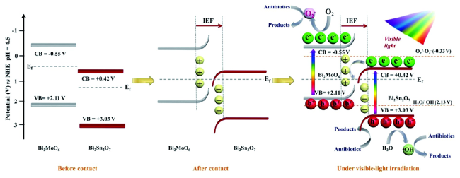
Photocatalysis is an attractive technology for clean energy production and environmental pollution prevention, which is of significant importance in promoting the realization of “carbon peaking and carbon neutral” in the future and adjusting the energy structure of China. However, among the various photocatalytic materials, bismuth-based catalysts with layered structures are of considerable attention in the field of photocatalysis owing to their suitable band gap. However, the photocatalytic activity of bismuth-based catalysts is limited by the lower separation and transport efficiency of carriers. This paper provides a summary of the strategies to enhance the photogenerated carrier separation and transport efficiency of bismuth-based catalysts through surface interface modulation, including morphology modulation, defect engineering, heteroatom doping and heterostructure construction. Particularly, the mechanism of the above strategies for improving the strength of the built-in electric field of bismuth-based catalysts, constructing efficient internal carrier transport channels and prolonging carrier lifetime is analyzed from the perspective of electronic structure and geometry. It provides a theoretical reference for further research on the design of catalysts with high carrier separation and transport efficiency. Finally, we analyzed the specific reasons for the improvement of carrier separation and transport efficiency by different surface interface strategies and the challenges and development prospects of bismuth-based catalysts in industrial applications.

Cite this article

Yixue Xu , Shishi Li , Xiaoshuang Ma , Xiaojin Liu , Jianjun Ding , Yuqiao Wang . Surface/Interface Modulation Enhanced Photogenerated Carrier Separation and Transfer of Bismuth-Based Catalysts[J]. Progress in Chemistry, 2023 , 35(4) : 509 -518 . DOI: 10.7536/PC220939

Contents

1 Introduction
2 Surface interface modulation strategy
2.1 Morphological control
2.2 Defect engineering
2.3 Heteroatom doping
2.4 Heterojunction construction
3 Conclusion and outlook

1 Introduction

At present, the sustainable development of human beings is facing two major problems: environmental pollution and energy shortage caused by the continuous consumption of fossil fuels. One of the challenges is to find technologies that can solve the two major crises of environment and energy. Among many new energy technologies, photocatalysis uses inexhaustible solar energy to develop new energy and eliminate environmental pollutants. Uch as photocatalytic water splitting, CO2 reduction, nitrogen fixation, organic synthesis, air purification, sterilization, organic pollutant removal and the like[1~6]. The sustainable, low-cost and efficient characteristics of photocatalytic technology make it one of the effective strategies to solve environmental problems and energy crisis.
The total catalytic efficiency of photocatalyst is determined by the light absorption efficiency of the catalyst, the separation and transfer efficiency of photogenerated carriers, and the surface catalytic reaction efficiency. Among them, photogenerated carriers refer to the electron-hole pairs generated in the semiconductor after photoexcitation, and their separation and transfer efficiency is the rate-determining step of the catalytic reaction. The surface and interface of the catalyst are important sites for carrier separation and transport, as well as for the adsorption and activation of reactant molecules to participate in the reaction. Therefore, the fine regulation of the surface and interface can effectively improve the reaction rate of the catalyst. Bismuth-based is a metallic element with low toxicity and radioactivity. Common classes are the binary bismuth-based semiconductors bismuth oxide (Bi2O3) and bismuth sulfide (Bi2S3). Ternary bismuth-based semiconductor bismuth tungstate (Bi2WO6), bismuth oxyhalide (BiOX (X = Cl, Br,Ⅰ)), bismuth oxycarbonate (Bi2O2CO3), bismuth ferrite (Bi2Fe4O9), and bismuth vanadate (BiVO4) as well as other bismuth-containing catalysts, such as bismuth titanate (Bi4Ti3O12), sodium bismuthate (NaBiO3) and bismuth oxyformate (BiOCOOH). The alternating anion-cation layered structure of bismuth-based semiconductors is beneficial to induce internal charges to form a Built-in electric field (IEF) through polarization[7~10]. The band gap of most bismuth-based catalysts remained within 3. 0 eV, showing good UV-Vis absorption ability[11]. Therefore, for bismuth-based catalysts, improving the efficiency of carrier separation and transfer is the key to enhance the catalytic activity.
In general, the photocatalytic reaction of photogenerated carriers mainly involves three steps: 1) the formation of electron-hole pairs inside the catalyst under photoexcitation; 2) electron-hole separation and migration to the surface active site to participate in the reaction; 3) Surface redox reaction consumes electrons or holes[12]. In the case of materials with good light absorption ability, improving the separation and migration rate of carriers can effectively activate the intrinsic activity of the catalyst. However, the vast majority of catalyst IEF is weak and cannot provide enough driving force to resist the binding of Coulomb force in the photocarrier separation process. In addition, the disordered migration of carriers, longer migration distance and shorter lifetime are also the main obstacles to the improvement of catalyst activity[13~15]. In this paper, we focus on the mechanism of surface and interface control strategies, such as morphology control, defect engineering, heteroatom doping and heterojunction construction, on the separation and transport of photogenerated carriers in bismuth-based catalysts. It provides a reference for the development of catalysts with high carrier transport efficiency from the perspective of regulating electronic and geometric structures. Finally, the challenges and prospects of bismuth-based catalysts in the future industrialization were summarized.

2 Surface and Interface Control Strategy

The surface and interface of catalyst are the key sites for molecular reaction, energy transfer, carrier separation and migration. Reasonable adjustment of the electronic structure and geometric structure of the surface and interface can effectively accelerate the carrier separation and transport efficiency, thereby improving the catalytic activity. As advanced characterization techniques reach atomic resolution, researchers can probe the process of charge generation, migration and recombination in the surface interface in more detail. The effects of surface and interface regulation on carrier transfer and separation are deeply analyzed at the microscopic scale to further guide the design and synthesis of catalysts.

2.1 Morphology control

Reasonable control of the atomic arrangement on the surface or interface of the catalyst can achieve the purpose of morphology control. The morphology of the catalyst has a significant effect on the crystal structure, band gap, specific surface area and light absorption capacity of the material. The design and synthesis of catalysts with different morphologies, such as ultrathin nanosheets, hollow nanospheres, hollow tubes, or hierarchical porous morphologies, can effectively adjust the geometric and electronic structures of the catalysts and affect the intrinsic activity of the catalysts.
The activity of the catalyst is proportional to the number of active sites on the surface, and a high specific surface area means that more active sites can be used to participate in the catalytic reaction. Therefore, Bi24O31Cl10 hollow spheres were synthesized by using carbonaceous microspheres as sacrificial templates[16]. The hollow structure provides a larger visible light absorption area, and the electrochemical test shows that the Bi24O31Cl10 hollow sphere has more excellent carrier separation and transmission efficiency, thereby having higher visible light catalytic degradation activity for rhodamine B. In addition, bismuth-rich hollow microspheres Bi4O5Br2 can be synthesized by one-step hydrothermal method without template[17]. Unlike the weak photocurrent response of BiOBr, the Bi4O5Br2 photocurrent response is significantly improved. In the Electrochemical impedance spectroscopy (EIS) test, the hollow microsphere Electrochemical impedance spectroscopy has smaller charge transfer resistance and faster carrier separation and migration (Fig. 1A, B). With the help of work function calculation, compared with BiOBr,Bi4O5Br2 hollow microspheres, electrons are more likely to spill over to the surface to participate in the reaction (Fig. 1C, d).
图1 (a)光电流响应图;(b)电化学阻抗图;(c,d)Bi4O5Br2和BiOBr的表面功函数[17]

Fig.1 (a) Photocurrent responses diagram; (b) electrochemical impedance plots; (c, d) the calculated surface work function of Bi4O5Br2 and BiOBr[17]. Copyright 2019, Elsevier

The ultrathin Bi4O5Br2 photocatalyst (3.7 nm) was synthesized by the glycerol precursor method, which is much lower than the thickness of BiOBr nanosheets (65 nm)[18]. The ultrathin strategy adjusts the charge density between the [Bi-O] layer and the double Br layer in Bi4O5Br2, causing polarization of the relevant orbitals and atoms, changing the direction of the IEF and improving its intensity. The driving electrons are transferred to the catalyst surface more quickly to participate in the reaction. One-dimensional Bi24O31Br10 nanoribbons formed unique Bi24O31Br10 hexagonal layered nanosheets upon ethylene glycol coordination induced dissolution-recrystallization (Fig. 2)[19]. The crossing and stacking of the nanosheets make the Bi24O31Br10 hexagonal nanoplates have more abundant interfaces, which effectively delays the recombination of electron-hole pairs and increases the number of electrons involved in the reaction by collecting bulk charges, which is beneficial to the improvement of the catalytic activity of the Bi24O31Br10 hexagonal layered nanoplates.
图2 不同Bi24O31Br10纳米结构的合成工艺[19]

Fig.2 Synthesis processes of different Bi24O31Br10 nanostructures[19]. Copyright 2019, Elsevier

One-dimensional catalysts have good crystallinity and stability, such as nanowires, nanotubes and nanorods. One-dimensional Bi2WO6 hollow tubes were synthesized by solvothermal method[20]. The formation of a layered structure from a solid tube to a hollow is shown in Figure 3A. The specific surface area of the Bi2WO6 hollow tube is increased by 58 times, and the hollow tube has good photocurrent response under the irradiation of a xenon lamp and smaller charge transfer resistance. The nanoscale thickness of the Bi2WO6 hollow tube facilitates charge transfer from the interior of the catalyst to the surrounding substrate, significantly improving carrier separation and transport rates.
图3 Bi2WO6的微棒结构到空心纳米管的演变过程示意图[20]

Fig.3 Schematic illustration of the evolution process from micro-rod structure to hollow nanotube Bi2WO6[20]. Copyright 2018, Elsevier

The bilayer structure of Bi12O17Cl2 ultrafine nanotubes has a distorted lattice, and the curved structure introduces oxygen defects[21]. The ultrathin structure provides a larger active area and shortens the carrier migration path. The EPR signal can be assigned to the electron "trapped" on the oxygen defect, increasing the probability of the electron participating in the reaction. The ultrathin tubular structure and oxygen deficiency synergistically accelerate carrier separation and migration.
In addition, catalysts with different exposure ratios of crystal planes can be obtained in the process of adjusting the morphology, and then photogenerated electrons and holes can be guided to aggregate on different crystal planes to achieve effective spatial separation. However, how to precisely control the exposed crystal plane is still one of the challenges in materials science. The strong covalent bonding within the layers of bismuth-based materials and the weak van der Waals interaction perpendicular to the layers endow the anisotropy of carrier transfer in different crystal planes. By CoOx (hole probe) and Ag (electron probe), the holes in BiOBr were spontaneously driven to the { 200 } surface by lateral IEF, and the electrons were driven to the { 001 } surface by vertical IEF[22]. The experimental results reveal that the IEFs manipulate the carrier transfer distance from 30 nm to 55 nm, and the electron diffusion length in the BiOBr catalyst is about 7 nm. In addition, Bi5O7I nanosheets with { 100 } and { 001 } as the main exposed facets were prepared by a combination of molecular precursor hydrolysis and calcination methods[23]. The conduction band position of Bi5O7I with exposed { 001 } facets is more negative and has stronger reduction ability. The electrochemical measurements showed that the Bi5O7I-001 has a higher photoinduced carrier separation efficiency than the Bi5O7I-100 facet. Therefore, controlling the exposure ratio of { 001 } crystal plane is an effective way to improve the carrier separation. The exposure ratio of { 010 }/{ 100 } facets of BiOIO3 nanosheets can be tuned by the variation of thickness[24]. Reducing the thickness along the [010] direction can promote the diffusion of carriers from the inside to the surface. Appropriate thickness can ensure the reasonable distribution of electrons on the { 010 } plane and holes on the { 100 } plane, and achieve efficient spatial separation of carriers.
Controlling the size and morphology of catalyst nanoparticles is an important means to develop new and efficient catalysts. Tuning the morphology of the catalyst can increase its specific surface area and thus improve the surface active sites. Tuning the fine structure of different surface atoms can optimize the electronic and geometric structure, shorten the carrier transfer path and improve the separation efficiency to enhance the catalytic activity.

2.2 Defect Engineering

Defect engineering optimizes the electronic structure of the catalyst by adjusting the surface microstructure to achieve rapid electron transfer and reduce the adsorption free energy of the substrate molecules. According to the scale, defects include point defects, line defects and surface defects. Defects can be divided into anion defects and cation defects according to their types. The formation of defects changes the physicochemical properties of the catalyst and is often used to improve the intrinsic activity of the catalyst.
Oxygen defect (OV) is a widely used anionic defect, which can induce energy levels with different depths in the band structure, increase the charge density, and induce the separation and transfer of photogenerated carriers[25]. Polyols were introduced during the hydrothermal process to construct BiO1-xBr/Bi2O2O3 with OV[26]. OV can be used as an electron mediator to guide the direction of photogenerated carriers and inhibit the recombination of carriers, and improve the photocatalytic activity of antibiotic degradation. In addition, in the Pd/BMO-SOV, the OV acts as an "electron bridge" to act as a built-in electric field[27]. When Pd/BMO-SOV is irradiated by blue light, the electrons generated by BMO-SOV will be transferred to Pd metal through the Schottky barrier induced by SOV, which promotes the effective separation of electron-hole pairs. Thus exhibiting excellent photocatalytic selective oxidation activity of aromatic alcohols (Fig. 4).
图4 在好氧和厌氧条件下可能发生的光催化选择性氧化反应途径[27]

Fig.4 Proposed possible photocatalytic selective oxidation reaction pathway under aerobic and anaerobic conditions[27]. Copyright 2021, Elsevier

Metal cation defects have the same promoting effect in the carrier separation process. The Bi2WO6 monolayer nanosheets with W defects (VW) were synthesized by a one-step hydrothermal method (Fig. 5A ∼ C)[28]. The introduction of subsurface VW can form a defect level, which not only broadens the visible light absorption region, but also acts as an electron capture center to suppress carrier recombination, leaving more holes on the surface of [BiO]+ to start the photocatalytic reaction (Figure 5D). BiOBr ultrathin nanosheets (VBi-BiOBr UNs) with abundant Bi defects (VBi) on the surface were synthesized by an ionic liquid-assisted method at room temperature[29]. The intermediate defect energy level generated by the VBi in the BiOBr nanosheet can make the conduction band shift negatively and enhance the oxidation ability. In addition, VBi modulates the electron local area, enhances the carrier concentration and accelerates the charge transfer. The incorporation of cationic vanadium defects (VV) in BiVO4 brings new defect levels and higher hole concentration near the Fermi level, which enhances the optical absorption and improves the electronic conductivity[30]. The increase of carrier lifetime from 74.5 ns to 143.6 ns was further confirmed by time-resolved fluorescence emission decay spectroscopy. The significantly increased fluorescence lifetime indicates that VV has a positive effect on the enhancement of carrier concentration.
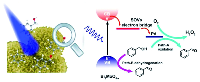
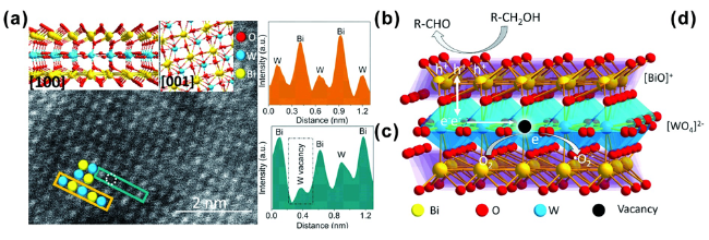
图5 (a)具有W缺陷的Bi2WO6的HAADF-STEM图像,插图中描述了其{100}和{001}晶面的原子结构;(b,c)沿HAADF-STEM图像中橙色框和绿色框的强度;(d)选择性光催化苄基醇氧化生成苯甲醛示意图[28]

Fig.5 (a) HAADF-STEM image of Bi2WO6 with W defects, inset depicting the atomic structure of its {100} and {001} crystal planes; (b, c) intensity of the orange and green boxes along the HAADF-STEM image; (d) schematic diagram of selective photocatalytic benzyl-alcohol oxidation of benzaldehyde[28]. Copyright 2020, American Chemical Society

Current research focuses on the influence of single defect on the electronic structure of materials, ignoring the synergistic effect of multiple defects. Therefore, OV and chlorine defects (ClV) were ingeniously introduced into BiOCl materials to explore the synergistic effect between the two defects. ClV transfers part of the localized electrons to the neighboring OV, making OV a center with "more abundant" electrons (Fig. 6a – d), which is beneficial to promote the chemisorption of O2 and its spontaneous dissociation into monatomic active oxygen (·O-), effectively oxidizing organic pollutants containing conjugated six-membered rings in the environment. The reason for the high activity can be attributed to the efficient electron capture and transfer by the chlorine-oxygen double defect[31].
图6 (a)BOC、(b)BOC-OV、(c)BOC-ClV和(d)BOC-(O+Cl)V表面电荷密度分布[31]

Fig.6 Surface charge density distribution of (a) BOC, (b) BOC-OV, (c) BOC-ClV and (d) BOC-(O+Cl)V[31]. Copyright 2022, American Chemical Society

The high-density defect energy level formed by the combination of OV and VBi can effectively reduce the band gap of Bi3O4Br[32]. Electrons are more likely to enter the CB level under thermal excitation (Fig. 7 a ~ d), and the defect-rich Bi3O4Br shows faster charge separation rate and longer fluorescence lifetime in femtosecond-resolved transient absorption spectroscopy and time-resolved transient photoluminescence spectroscopy tests (Fig. 7 e, f).
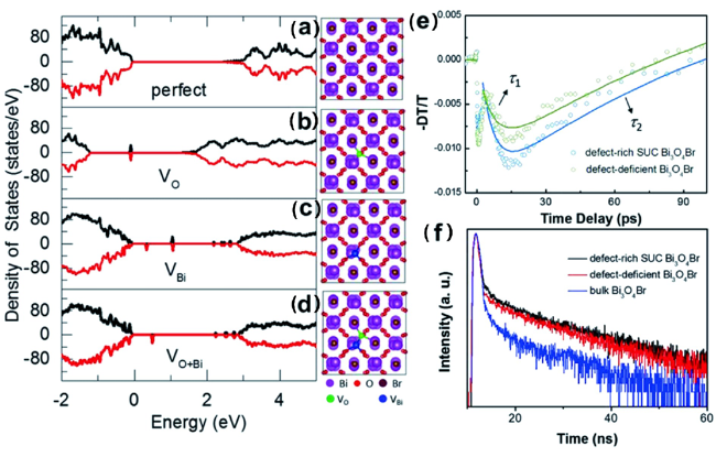
图7 (a~d)Bi3O4Br、Bi3O4Br含一个氧空位、Bi3O4Br含一个铋空位、Bi3O4Br含一个铋空位和一个氧空位的态密度计算;(e)飞秒分辨瞬态吸收光谱和(f)时间分辨瞬态荧光光谱[32]

Fig.7 (a~d) Density of states calculations for Bi3O4Br, Bi3O4Br with one oxygen vacancy, Bi3O4Br with one bismuth vacancy, and Bi3O4Br with one bismuth vacancy and one oxygen vacancy; (e) ultrafast TA spectroscopy and (f) time-resolved transient PL decay[32]. Copyright 2019, Wiley

To sum up, the introduction of anionic or cationic defects can adjust the electronic structure of the catalyst, and the formation of defect intermediate levels can increase the local electron density for capturing photogenerated electrons, effectively inhibiting the recombination of carriers and prolonging the lifetime of carriers[33,34]. In addition, double defects form defect channels through defect-defect and defect-electron interactions, which promote the improvement of electronic conductivity and the separation of photogenerated electron-hole pairs, thus improving the intrinsic activity of the catalyst[35,36].

2.3 Heteroatom doping

The introduction of metal or nonmetal ions into the semiconductor can adjust the electronic structure and geometric structure of the catalyst, effectively change the transfer pathway of carriers, and is essential to improve the electron-hole separation efficiency of a single semiconductor[37~40]. Among them, nonmetal doping increases the active sites and improves the electronic conductivity and charge transfer kinetics. Metal doping changes the electronic structure and the local binding environment of the pristine material. Both regulate the intrinsic properties of the semiconductor to some extent.
Nonmetal C doping is often used to enhance the carrier separation efficiency. The introduction of C into the lattice of Bi3O4Cl induces non-uniform charge distribution polarization, which enhances the IEF by 126 times and the volume charge separation efficiency by 80%[41]. The enhanced IEF will drive the transfer and enrichment of electrons and holes within the [Bi3O4] and [Cl] sheets of Bi3O4Cl, respectively, reducing the recombination rate. Higher IEF enables more electrons and holes to be separated from the bulk and transferred to the surface, and provides a stronger ability to constrain recombination (Fig. 8). In addition, doping C in ultrathin Bi2MoO6 nanosheets can effectively adjust the energy band structure of the catalyst, broaden the band gap of the catalyst, and hinder the recombination of photogenerated carriers. Doped C can also act as a springboard for photocarrier separation, inducing electron transfer from the interior to the surface[42].
图8 纯Bi3O4Cl和C掺杂Bi3O4Cl中电子和空穴的分离和迁移示意图[41]

Fig.8 Schematic illustration of the separation and migration of electrons and holes in pure Bi3O4Cl and C-doped Bi3O4Cl[41]. Copyright 2016, Wiley

Non-metal B was doped into BiOCl nanosheets by molten salt strategy[43]. Bulk B-doping may mitigate the strong exciton effect confined in BiOCl by reducing the binding energy (Eb) of the exciton, thereby accelerating the dissociation of bulk excitons into electron-holes (Figure 9). Meanwhile, the B doping on the surface can reconstruct the surface of atomic-scale BiOCl and generate B-O defects (B-OV), thus realizing the spontaneous activation of CO2, inhibiting competitive hydrogen evolution, and promoting the selective generation of CO from CO2. As a result, the rate of CO2-CO conversion was increased to 83.64μmol·g-1·h-1, and the reactivity could be maintained for more than 120 H under visible light.
图9 B体相掺杂对BiOCl-B-OV激子解离和载流子产生的影响示意图[43]

Fig.9 Schematic illustration of the effect of B doping on BiOCl-B-OV excitons dissociation and carrier generation[43]. Copyright 2021, Wiley

Transition metal ions as dopants can create lattice defects in semiconductors or change the crystal structure to avoid electron-hole recombination. For example, the BiOBr/PVP microspheres doped with Zn2+ can effectively reduce the recombination rate of photogenerated electron-hole pairs under visible light, resulting in enhanced photocatalytic activity[44]. In addition, transition metal self-doping can tune the crystal and electronic structure of Bi2WO6. Bi atom replaced W atom to prepare Bi2+xWO6[45]. The Bader charge of oxygen atoms around the substituted Bi atom in Bi2+xWO6 slightly decreased compared with that in the pristine Bi2WO6, indicating that the dopant redistributed the charge around Bi2+xWO6. This redistribution will change the IEF, which is beneficial for better separation of photogenerated carriers, thus improving the photocatalytic activity of Bi2+xWO6 under visible light.
Among many dopants, single-atom catalysts have attracted much attention in different types of chemical reactions because of their high atom utilization and catalytic activity. The electronic structure of the active site on the catalyst surface can be controlled by precisely adjusting the coordination environment of different atoms. Among them, the type of single atom, the electronic configuration, the number of electrons in the d orbital and the energy level have a profound impact on the separation and transmission of catalyst carriers[46,47]. Therefore, the selection of the appropriate central atom is very important for the catalytic activity and selectivity of the catalyst. In Co-Bi3O4Br, Co atoms replace Bi atoms in the lattice[48]. The Fourier transform (FT)k3 weighted EXAFS spectrum verified that Co was distributed as a single atom. Ultrafast transient absorption spectroscopy was used to study the dynamic behavior of photogenerated carriers, and Co single atoms provide trap States to capture more photogenerated electrons and prolong the lifetime of carriers, which provides more opportunities for CO2 photoreduction. In addition, the average fluorescence lifetime and surface photovoltage intensity of Co-Bi3O4Br are much higher than those of Bi3O4Br, which further illustrates the improvement of carrier separation efficiency in Co-Bi3O4Br.
Implanting monatomic Fe into the lattice of Bi4O5I2 by a simple solvothermal method can effectively prevent the agglomeration of monatomic Fe (Fig. 10a)[49]. The introduction of single-atom Fe modulates the electronic structure of the catalyst. The band distribution of Bi4O5I2-Fe30 is more dense than that of Bi4O5I2 intrinsic band, and a small number of impurity levels appear near the conduction band edge (Fig. 10 B). Bi4O5I2-Fe30 has a smaller work function, which means that the single atom acts as a springboard for one electron transition, making it easier for the electron to overcome the Coulomb force and transfer to the surface to participate in the reaction (Fig. 10 C, d).
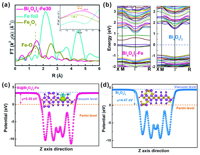
图10 (a)Bi4O5I2-Fe30的Fe K边缘扩展XANES振荡函数k3χ(k)和EXAFS;(b)Bi4O5I2-Fe30和Bi4O5I2能带结构的计算;(c)Bi4O5I2-Fe30和(d)Bi4O5I2的表面功函数计算[49]

Fig.10 (a) Fe K-edge extended XANES oscillation functions k3χ(k) and EXAFS spectra of Bi4O5I2-Fe30; (b) The calculated band structures; the calculated surface work function of Bi4O5I2-Fe30 and Bi4O5I2, (c) Bi4O5I2-Fe30 and (d) Bi4O5I2[49]. Copyright 2021, American Chemical Society

The electron transfer behavior of Pt/BiOBr { 001 } photocatalytic system was investigated by theoretical calculation[50]. Surface work function: Pt (5.650 eV) > BiOBr { 001 } (2.576 eV), therefore, the photogenerated electrons flow directionally from BiOBr onto single-atom Pt. When the Fermi level height of the two reaches the same level, the energy band will bend and the loss layer will appear on the contact surface. The Schottky barrier generated between the two ensures the unidirectional flow of electrons between the interfaces and effectively prevents the recombination of photogenerated carriers.
In particular, surface halogenation is a special doping method. The Bi2O2(OH)(NO3) nanosheets with halogen ions (Cl-,Br- and I-) grafted on Bi atoms in situ are efficient Sill Sill Én-phased layer structure photocatalysts, which can introduce surface polarization and effectively guide the separation of bulk charge from surface charge. In addition, surface halogenation favors the activation of hydroxyl groups, promoting the adsorption of CO2 molecules/protons on these reaction sites and the CO2 conversion reaction[51].
Doping strategy is an effective way to tune the band structure, light absorption ability, and substrate adsorption and activation free energy of catalysts. The coordinatively unsaturated dopant atoms with high activity can effectively capture electrons and quickly transfer them to the adsorbed substrate, thus improving the utilization of carriers. Among them, single-atom doping can also be used as an electron springboard to improve the separation and transport rate of carriers, thus improving the activity of the catalyst.

2.4 Build heterojunction

Heterojunction constructed by two semiconductor materials with matching parameters is a powerful tool to manipulate the interfacial properties and electronic structure of catalysts. The types of heterojunction include p-n junction, Schottky junction, traditional heterojunction (straddle type, staggered type and gap type), Z-type heterojunction and van der Waals heterojunction[52~54]. Reasonable selection of semiconductor materials with matched lattice parameters and construction strategies can effectively control the electronic structure to construct the internal transport electric field, so that carriers can be transported and separated efficiently and orderly.
The junction formed by an n-type semiconductor providing electrons and a p-type semiconductor providing holes is a p-n heterojunction. At the interface of the BiOI/Bi2O2SO4p-n heterojunction, IEF induced the establishment of an electron transport channel[55]. The electron-rich interfacial environment promotes the activation of reactants and the generation of reactive oxygen species, preventing the formation of toxic by-products (Fig. 11). Similar to the p-n heterojunction, there is a contact potential difference between the Ti3C2Tx and the Bi2S3, resulting in a Bi2S3/Ti3C2Tx interface Schottky junction[56]. The different work functions lead to the formation of local electrophilic/nucleophilic regions. Self-driven charge transfer across the interface onto Ti3C2Tx increases its local electron density. The formed Schottky barrier suppresses the backflow of electrons and facilitates the charge transfer and separation.
图11 BiOI/Bi2O2SO4 p-n异质结形成示意图[55]

Fig.11 Schematic illustration of the BiOI/Bi2O2SO4 p-n heterojunction[55]. Copyright 2022, Elsevier

Type-Ⅱ heterojunction is one of the most studied heterojunctions because of its efficient interface transfer and spatial separation of electron-hole pairs under photoexcitation. For example, the BiOIO3/MoS2 heterojunction belongs to the staggered type type-II heterojunction[57]. Photoexcitation causes the electron generated by RhB to be transferred to the CB of MoS2 and further transported to the CB of BiOIO3. The hole is transferred from the VB of BiOIO3 to the VB of MoS2. The electrons and holes are accumulated on BiOIO3 and MoS2, respectively, which improves the separation efficiency of photoinduced carriers and enhances the photocatalytic performance.
Although the introduction of IEF into Type-II heterojunction constructs the electron-hole transport channel, it improves the carrier separation efficiency in a certain range. However, it is premised on the sacrifice of partial redox capacity. Therefore, Z-type heterojunction emerges as the times require. It simulates the photosynthesis of plants in nature and has high carrier separation efficiency without sacrificing redox capacity[58]. A closely linked Z-shaped heterojunction was formed between the 2D/2D BP/MBWO nanosheets (Fig. 12)[59]. The VB and CB of MBWO and BP nanosheets generated holes and electrons under visible light irradiation. The electron transport channel inside the heterojunction makes the electron of CB in MBWO combine with the hole of VB in BP, and the electron of BP reduces O2 to the hole of ·O2-,MBWO and oxidizes H2O to · OH. ·O2- and · OH further oxidized NO to NO 3 -, and the NO removal rate was as high as 67%. This can be attributed to the interfacial cooperative effect of 2D/2D heterojunction, efficient charge separation and transfer, and strong light absorption. It is interesting to further introduce metal Bi as an intermediate bridge on the basis of the Z-shaped photocatalyst Bi2O3/KTN, which can more closely connect the two catalysts and transport electrons directionally to achieve the purpose of inhibiting carrier recombination[60]. Metal Bi also promotes the adsorption and activation between KTN and N2, effectively reducing the competitive HER and improving the NRR efficiency. Transverse photogenerated electron-hole transport by BiOCl@Bi2O3 through an internal electric field induced by a lateral interfacial chemical bond. Compared with BiOCl, the electron density distribution of O in the [Bi2O2]2+ slab of BiOCl@Bi2O3 at the heterointerface prefers to be partially oriented toward the edge. This indicates that BiOCl@Bi2O3 has a stronger chemical bond, and this stronger chemical bond induces a stronger internal electric field, which contributes to better photoexcited charge separation and charge transfer kinetics[61]. In addition, the formation of Z-type system The chemical bond between the interfacial Co — O-W between Bi2WO6 and CoPc facilitates the built-in electric field, which promotes the charge separation and maintains a high redox potential. At the same time, the Co-N4(Ⅱ) site of CoPc can act as an enhanced electron pump to capture more electrons from the ligand after photoexcitation and promote the Z-shaped charge transfer of the CoPc/Bi2WO6 composite, and it can also act as a O2 activation site to consume electrons, reduce oxygen, and generate ·O2- radicals[62]. The construction of heterostructures can bring adjacent components into contact at the atomic level, resulting in a large number of chemical bonds[63]. The chemical bond between the interfaces is a bridge between the interfacial space charge regions, which can promote the formation of the built-in electric field and accelerate the electron-hole transfer.
图12 BP/MBWO异质结的制备说明示意图[59]

Fig.12 Illustration of the fabrication of the BP/MBWO heterojunction[59]. Copyright 2019, Wiley

In 2019, Yu et al. Proposed the concept of S-type heterojunction on the basis of Z-type heterojunction[64]. The reduced semiconductor photocatalyst (RP) has a high Fermi level and a small work function, while the oxidized semiconductor photocatalyst (OP) has a low Fermi level and a large work function. The S-type heterojunction formed by the two staggered structures can achieve efficient carrier separation (fig. 13). The biggest difference from the Z-type heterojunction is that the Fermi levels of the two semiconductors are arranged at the same energy level. This makes the band bending of OP and RP, and the electrostatic attraction promotes the electron-hole recombination at the interface between OP and RP, and the electron-hole remains in the conduction band of RP and the valence band of OP, respectively, thus having efficient electron-hole separation and redox ability.
图13 (a)接触前,(b)接触后,(c)S-异质结中光生载流子转移过程[64]

Fig.13 (a) Before contact, (b) after contact, (c) photogenerated charge carrier transfer process in S-scheme mode[64]. Copyright 2020, Elsevier

The Bi2Sn2O7/Bi2MoO6S-type heterojunction is constructed by combining Bi2Sn2O7 nanoparticles with Bi2MoO6 microspheres,The existing IEF between the interface of Bi2MoO6 and Bi2Sn2O7 makes the energy band of Bi2Sn2O7 bend downward due to the accumulation of electrons, and the energy band of Bi2MoO6 bend upward due to the loss of electrons[65]. Therefore, the presence of IEF builds an internal transport channel for the transfer of photogenerated electrons from Bi2Sn2O7 to Bi2MoO6, effectively improving the separation and transport efficiency of carriers (Fig. 14).
图14 提出了可见光下Bi2Sn2O7/Bi2MoO6 S-异质结的光催化改善机理[65]

Fig.14 Proposed photocatalysis improvement mechanism of the Bi2Sn2O7/Bi2MoO6 S-scheme heterojunction under visible light[65]. Copyright 2022, Elsevier

Different two-dimensional atomic layers can be stacked in a set order by means of weak van der Waals force to form a heterojunction structure with an atomically flat interface, which maintains the original ultra-thin characteristics. Such heterostructures are often referred to as van der Waals heterojunctions. In the Bi3O4Cl/g-C3N4vdW heterojunction, both belong to the 2D structure, and there is a weak van der Waals force between the layers, which provides a basis for the construction of van der Waals heterojunction[66]. The formation of Bi3O4Cl/g-C3N4vdW heterojunction avoids the problems of lattice defects and catalyst quality degradation caused by the combination of traditional catalysts. The electrostatic attraction between the layers accelerates the charge separation and transport at the interface, and effectively reduces the electron-hole recombination rate and prolongs the carrier lifetime. This strategy can effectively avoid the problems of poor lattice matching and poor stability. In addition, thanks to the two-dimensional structure of bismuth-based materials, BiOCl itself can generate van der Waals forces internally through the vapor exfoliation method, and the layers are parallel and adjacent to each other[67]. The interstices of Cl atoms interacting via van der Waals forces are mapped between two adjacent [Bi2O2] layers. Increasing the VDWG fraction from 76% to 99% reduces the exciton confinement energy Eb from 137 meV to 36 meV, thereby increasing the bulk charge separation efficiency by a factor of 50.
The construction of heterojunction avoids the disadvantage of poor carrier spatial separation ability of traditional catalysts. It is an effective strategy to improve the electron-hole separation and redox ability of catalysts by introducing carrier transport channels inside and at the interface of catalysts to induce the separation and aggregation of electron-hole directional order and participate in surface reactions.

3 Summary and Prospect

In this paper, we focus on the key issues of bismuth-based materials in the separation and transport of photogenerated carriers, and review the positive effects of different surface and interface strategies, such as morphology control, defect engineering, heteroatom doping, and heterojunction construction, on the electronic structure and geometric structure of materials. The reasons for the effective improvement of carrier transport and transfer efficiency can be summarized into four aspects: (1) The surface and interface strategy adjusts the band gap width and increases the intermediate energy level, reduces the binding of Coulomb force on carriers, and increases the carrier concentration; (2) The adjustment of surface local electronic structure and the formation of unsaturated active sites can act as "traps" to capture electron-hole, reduce the recombination rate and prolong the carrier lifetime; (3) The surface and interface strategy adjusts the geometric structure of the catalyst, shortens the migration path of carriers, and reduces the probability of carrier recombination; (4) The surface and interface strategy constructs a special carrier transport channel, which induces electron-hole directional migration and enrichment to the conduction band and valence band of the catalyst to participate in the reaction, thus improving the utilization of carriers. At present, bismuth-based catalysts have a certain theoretical basis in the field of photocatalysis, but there are some problems to be solved in the future industrial development process: (1) The time scale of charge migration process is usually between femtoseconds and picoseconds.In-situ dynamic and high-resolution characterization methods need to be further developed to reveal the effects of surface and interface strategies on carrier concentration, transport path and transport rate, so as to better guide the production and application of efficient industrial catalysts. (2) The active sites in the photocatalytic process are heterogeneous and dynamically evolve with the change of the reaction environment. Exploring the evolution law of catalyst surface and interface microstructure plays a positive guiding role in the design of efficient industrial catalysts. (3) The valence band position of bismuth-based catalyst determines its advantages in photocatalytic degradation of pollutants and sterilization. However, the lower conduction band position limits the development of bismuth-based materials in organic synthesis and photocatalytic hydrogen production. Therefore, it is very important to expand the industrial application range of the catalyst. (4) The preparation methods of bismuth-based catalysts mainly include hydrothermal method, solid phase method, precursor method and so on. The complex preparation process and small output hinder the industrialization process. In the following exploration, we will focus on the improvement of preparation methods and the control of raw material costs, and improve the cycle stability and practical application efficiency of catalysts to promote their industrialization process.
[1]
Ma Y, Wang X L, Jia Y S, Chen X B, Han H X, Li C. Chem. Rev., 2014, 114(19): 9987.

[2]
Di J, Xia J X, Li H M, Guo S J, Dai S. Nano Energy, 2017, 41: 172.

[3]
Ouyang T, Wang H J, Huang H H, Wang J W, Guo S, Liu W J, Zhong D C, Lu T B. Angew. Chem. Int. Ed., 2018, 57(50): 16480.

[4]
Kominami H, Yamamoto S, Imamura K, Tanaka A, Hashimoto K. Chem. Commun., 2014, 50(35): 4558.

[5]
Yang X F, Qin J L, Jiang Y, Chen K M, Yan X H, Zhang D, Li R, Tang H. Appl. Catal. B Environ., 2015, 166: 231.

[6]
Xia D H, Liu H D, Xu B H, Wang Y C, Liao Y H, Huang Y J, Ye L Q, He C, Wong P K, Qiu R L. Appl. Catal. B Environ., 2019, 245: 177.

[7]
Guan Y, Wu J, Lin Y Y, Liu Q Z, Qi Y F, Pan W G, He P, Qi X M, Wang R, Ji Z H. Appl. Surf. Sci., 2019, 481: 838.

[8]
Guan Y, Wu J, Man X K, Liu Q Z, Qi Y F, He P, Qi X M. Chem. Eng. J., 2020, 396: 125234.

[9]
Kim T W, Choi K S. Science, 2014, 343(6174): 990.

[10]
Fan Z, Zhao Y B, Zhai W, Qiu L, Li H, Hoffmann M R. RSC Adv., 2016, 6(3): 2028.

[11]
Zhang K, Wang J, Jiang W J, Yao W Q, Yang H P, Zhu Y F. Appl. Catal. B Environ., 2018, 232: 175.

[12]
Kudo A, Miseki Y. Chem. Soc. Rev., 2009, 38(1): 253.

[13]
Chen L X. PANS, 2020, 117(16): 8672.

[14]
Li L, Salvador P A, Rohrer G S. Nanoscale, 2014, 6(1): 24.

[15]
Xiong J, Di J, Li H M. Adv. Sci., 2018, 5(7): 1800244.

[16]
Cui P Z, Wang J L, Wang Z M, Chen J, Xing X R, Wang L Z, Yu R B. Nano Res., 2016, 9(3): 593.

[17]
Jin X L, Lv C D, Zhou X, Xie H Q, Sun S F, Liu Y, Meng Q Q, Chen G. Nano Energy, 2019, 64: 103955.

[18]
Ye L Q, Jin X L, Liu C, Ding C H, Xie H Q, Chu K H, Wong P K. Appl. Catal. B Environ., 2016, 187: 281.

[19]
Chen X, Zhang J, Liu L, Hu B R, Zhao Y L, Zhao S, Zhao W T, Li S, Hai X. Appl. Surf. Sci., 2019, 491: 1.

[20]
Xiao L B, Lin R B, Wang J, Cui C, Wang J Y, Li Z Q. J. Colloid Interface Sci., 2018, 523: 151.

[21]
Di J, Zhu C, Ji M X, Duan M L, Long R, Yan C, Gu K Z, Xiong J, She Y B, Xia J X, Li H M, Liu Z. Angew. Chem. Int. Ed., 2018, 57(45): 14847.

[22]
Luo Z S, Ye X Y, Zhang S J, Xue S K, Yang C, Hou Y D, Xing W D, Yu R, Sun J, Yu Z Y, Wang X C. Nat. Commun., 2022, 13: 2230.

[23]
Bai Y, Ye L Q, Chen T, Wang L, Shi X, Zhang X, Chen D. ACS Appl. Mater. Interfaces, 2016, 8(41): 27661.

[24]
Chen F, Huang H W, Ye L Q, Zhang T R, Zhang Y H, Han X P, Ma T Y. Adv. Funct. Mater., 2018, 28(46): 1804284.

[25]
Sun M L, Dong X A, Lei B, Li J Y, Chen P, Zhang Y X, Dong F. Nanoscale, 2019, 11(43): 20562.

[26]
Ding J, Dai Z, Qin F, Zhao H P, Zhao S, Chen R. Appl. Catal. B Environ., 2017, 205: 281.

[27]
Sun Z L, Yang X L, Yu X F, Xia L H, Peng Y H, Li Z, Zhang Y, Cheng J B, Zhang K S, Yu J Q. Appl. Catal. B Environ., 2021, 285: 119790.

[28]
Huang H W, Zhou C, Jiao X C, Yuan H F, Zhao J W, He C Q, Hofkens J, Roeffaers M B J, Long J L, Steele J A. ACS Catal., 2020, 10(2): 1439.

[29]
Di J, Chen C, Zhu C, Song P, Xiong J, Ji M X, Zhou J D, Fu Q D, Xu M Z, Hao W, Xia J X, Li S Z, Li H M, Liu Z. ACS Appl. Mater. Interfaces, 2019, 11(34): 30786.

[30]
Gao S, Gu B C, Jiao X C, Sun Y F, Zu X L, Yang F, Zhu W G, Wang C M, Feng Z M, Ye B J, Xie Y. J. Am. Chem. Soc., 2017, 139(9): 3438.

[31]
Yang Z P, Shi Y B, Li H, Mao C L, Wang X B, Liu X F, Liu X, Zhang L Z. Environ. Sci. Technol., 2022, 56(6): 3587.

[32]
Di J, Xia J X, Chisholm M F, Zhong J, Chen C, Cao X Z, Dong F, Chi Z, Chen H L, Weng Y X, Xiong J, Yang S Z, Li H M, Liu Z, Dai S. Adv. Mater., 2019, 31(28): 1807576.

[33]
Li L Q, Long R, Bertolini T, Prezhdo O V. Nano Lett., 2017, 17(12): 7962.

[34]
Zhou W, Fu H G. Inorg. Chem. Front., 2018, 5(6): 1240.

[35]
Xu Y C, Li H Z, Sun B J, Qiao P Z, Ren L P, Tian G H, Jiang B J, Pan K, Zhou W. Chem. Eng. J., 2020, 379: 122295.

[36]
Bai S, Zhang N, Gao C, Xiong Y J. Nano Energy, 2018, 53: 296.

[37]
Li Z A, Wang J L, Chen J F, Liu L, Yang X F, Chen T, Chen Z Z, Yang M M, Yan W S, Fu Z P, Liu M, Lu Y L. J. Alloys Compd., 2019, 806: 492.

[38]
Ikram M, Hassan J, Raza A, Haider A, Naz S, Ul-Hamid A, Haider J, Shahzadi I, Qamar U, Ali S. RSC Adv., 2020, 10(50): 30007.

[39]
Wang S, Bai L M, Ao X L. RSC Adv., 2018, 8(64): 36745.

[40]
Wang Y Q, Xu X X, Lu W, Huo Y Q, Bian L J. Dalton Trans., 2018, 47(12): 4219.

[41]
Li J, Cai L J, Shang J, Yu Y, Zhang L Z. Adv. Mater., 2016, 28(21): 4059.

[42]
Wang S Y, Ding X, Zhang X H, Pang H, Hai X, Zhan G M, Zhou W, Song H, Zhang L Z, Chen H, Ye J H. Adv. Funct. Mater., 2017, 27(47): 1703923.

[43]
Shi Y B, Zhan G M, Li H, Wang X B, Liu X F, Shi L J, Wei K, Ling C C, Li Z L, Wang H, Mao C L, Liu X, Zhang L Z. Adv. Mater., 2021, 33(38): 2100143.

[44]
Zhou J, Zhou J B, Hu Z S, Wang L. Mater. Sci. Semicond. Process., 2019, 90: 112.

[45]
Ding X, Zhao K, Zhang L Z. Environ. Sci. Technol., 2014, 48(10): 5823.

[46]
Jin X X, Wang R Y, Zhang L X, Si R, Shen M, Wang M, Tian J J, Shi J L. Angew. Chem. Int. Ed., 2020, 59(17): 6827.

[47]
Wang Q, Li J, Tu X. Chem. Mater., 2019, 32: 734.

[48]
Di J, Chen C, Yang S Z, Chen S M, Duan M L, Xiong J, Zhu C, Long R, Hao W, Chi Z, Chen H L, Weng Y X, Xia J X, Song L, Li S Z, Li H M, Liu Z. Nat. Commun., 2019, 10: 2840.

[49]
Jin X L, Xu Y X, Zhou X, Lv C D, Huang Q Z, Chen G, Xie H Q, Ge T, Cao J, Zhan J Q, Ye L Q. ACS Mater. Lett., 2021, 3(4): 364.

[50]
Zhang X C, Guan M H, Zhang Q R, Zhang C M, Li R, Liu J X, Wang Y W, Fan C M, Acta Phys. Sin., 2021, 70(8): 087101.

张小超, 管美画, 张启瑞, 张长明, 李瑞, 刘建新, 王雅文, 樊彩梅. 物理学报, 2021, 70(8): 087101.).

[51]
Hao L, Kang L, Huang H W, Ye L Q, Han K L, Yang S Q, Yu H J, Batmunkh M, Zhang Y H, Ma T Y. Adv. Mater., 2019, 31(25): 1900546.

[52]
Xie M Z, Fu X D, Jing L Q, Luan P, Feng Y J, Fu H G. Adv. Energy Mater., 2014, 4(5): 1300995.

[53]
Wang M Y, Sun L, Lin Z Q, Cai J H, Xie K P, Lin C J. Energy Environ. Sci., 2013, 6(4): 1211.

[54]
Yu J G, Low J, Xiao W, Zhou P, Jaroniec M. J. Am. Chem. Soc., 2014, 136(25): 8839.

[55]
Geng Q, Xie H T, He Y, Sun Y J, Hou X F, Wang Z M, Dong F. Appl. Catal. B Environ., 2021, 297: 120492.

[56]
Li J F, Li Z Y, Liu X M, Li C Y, Zheng Y F, Yeung K W K, Cui Z D, Liang Y Q, Zhu S L, Hu W B, Qi Y J, Zhang T J, Wang X B, Wu S L. Nat. Commun., 2021, 12: 1224.

[57]
Lu M L, Xiao X Y, Wang Y, Chen J Y. J. Alloys Compd., 2020, 831: 154789.

[58]
Kosco J, Bidwell M, Cha H, Martin T, Howells C T, Sachs M, Anjum D H, Gonzalez Lopez S, Zou L Y, Wadsworth A, Zhang W M, Zhang L S, Tellam J, Sougrat R, Laquai F, DeLongchamp D M, Durrant J R, McCulloch I. Nat. Mater., 2020, 19(5): 559.

[59]
Hu J D, Chen D Y, Mo Z, Li N J, Xu Q F, Li H, He J H, Xu H, Lu J M. Angew. Chem., 2019, 131(7): 2095.

[60]
Chen L, Wang J F, Li X J, Zhao C R, Hu X, Wu Y, He Y M. Inorg. Chem. Front., 2022, 9(11): 2714.

[61]
Wang L, Zhao X, Lv D D, Liu C W, Lai W H, Sun C Y, Su Z M, Xu X, Hao W C, Dou S X, Du Y. Adv. Mater., 2020, 32(48): 2004311.

[62]
Li G J, Lian Z, Wan Z W, Liu Z N, Qian J W, Deng Y, Zhang S L, Zhong Q. Appl. Catal. B Environ., 2022, 317: 121787.

[63]
Chen W X, Wei W, Wang K F, Zhang N, Chen G L, Hu Y J, Ostrikov K K. Nanoscale, 2021, 13(12): 6201.

[64]
Xu Q L, Zhang L Y, Cheng B, Fan J J, Yu J G. Chem, 2020, 6(7): 1543.

[65]
Li S J, Wang C C, Liu Y P, Cai M J, Wang Y N, Zhang H Q, Guo Y, Zhao W, Wang Z H, Chen X B. Chem. Eng. J., 2022, 429: 132519.

[66]
Xu Y X, Jin X L, Ge T, Xie H Q, Sun R X, Su F Y, Li X, Ye L Q. Chem. Eng. J., 2021, 409: 128178.

[67]
Shi Y B, Li J, Mao C L, Liu S, Wang X B, Liu X F, Zhao S X, Liu X, Huang Y Q, Zhang L Z. Nat. Commun., 2021, 12: 5923.

Outlines

/