Home Journals Progress in Chemistry
Progress in Chemistry

Abbreviation (ISO4): Prog Chem      Editor in chief: Jincai ZHAO

About  /  Aim & scope  /  Editorial board  /  Indexed  /  Contact  / 
Review

Modification and Application of Bi2MoO6 in Photocatalytic Technology

  • Dandan Wang , 1, 2, * ,
  • Zhaoxin Lin 3, 4 ,
  • Huijie Gu 3, 4 ,
  • Yunhui Li 3, 4 ,
  • Hongji Li , 1, 2, * ,
  • Jing Shao , 3, 4, *
Expand
  • 1. College of Engineering, Jilin Normal University,Siping 136000, China
  • 2. Key Laboratory of Preparation and Application of Environmental Friendly Materials (Jilin Normal University), Ministry of Education,Changchun 130103, China
  • 3. School of Chemistry and Environmental Engineering, Changchun University of Science and Technology,Changchun 130022, China
  • 4. Zhongshan Institute of Changchun University of Science and Technology,Zhongshan 528437, China
* Corresponding author e-mail: (Dandan Wang);
(Hongji Li);
(Jing Shao)

Received date: 2022-09-29

  Revised date: 2023-01-30

  Online published: 2023-02-20

Supported by

development of Science and Technology of Jilin Province(YDZJ202201ZYTS629)

Natural Science Foundation Project of Jilin Province(YDZJ202201ZYTS356)

Natural Science Foundation Project of Jilin Province(YDZJ202101ZYTS073)

Abstract

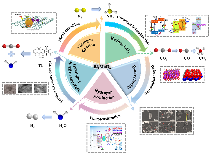
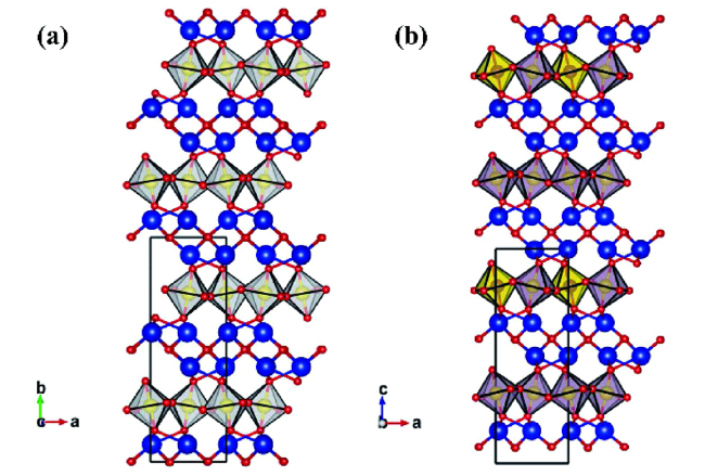
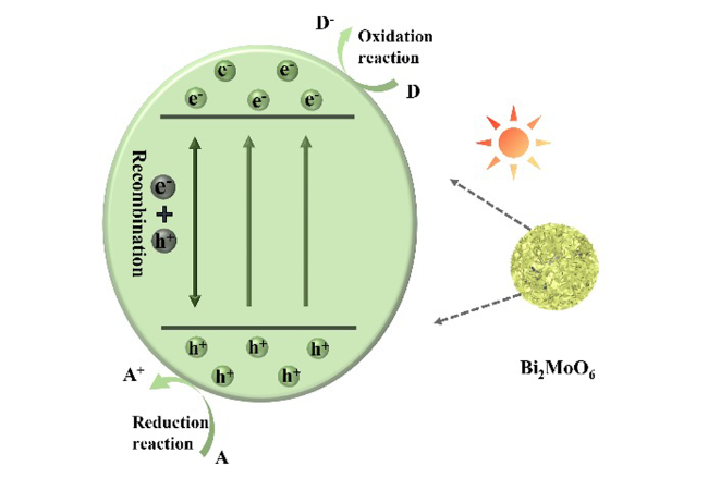
At present, ecological pollution and energy shortage have become global problems threatening human survival. Green and low energy consumption photocatalytic technology is of strategic significance to solve environmental disaster and energy crisis. As a ternary Aurivillius compound, Bi2MoO6 has attracted extensive attention of researchers due to its unique layered structure. However, the high carrier recombination rate limits its application in photocatalysis. This paper summarizes the strategies for modifying the performance of Bi2MoO6 based photocatalysts, such as surface structure tuning, defect engineering, metal deposition, heterojunction fabrication and photosensitization treatment. In many modification strategies, the influence of the construction of Bi2MoO6 based heterojunction on the photocatalytic performance has been mainly discussed. Finally, the current challenges faced by Bi2MoO6 based photocatalyst in photocatalysis technology are summarized, and the future development prospects are given, providing new ideas for accelerating the development of Bi2MoO6 based photocatalyst.

Cite this article

Dandan Wang , Zhaoxin Lin , Huijie Gu , Yunhui Li , Hongji Li , Jing Shao . Modification and Application of Bi2MoO6 in Photocatalytic Technology[J]. Progress in Chemistry, 2023 , 35(4) : 606 -619 . DOI: 10.7536/PC220934
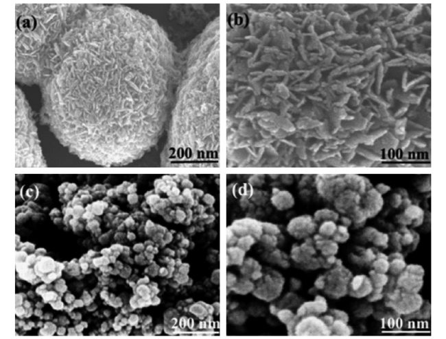
Contents

1 Introduction
2 Preparation method
2.1 Hydrothermal/Solvothermal method
2.2 High temperature solid phase method
2.3 Coprecipitation method
2.4 Template method
2.5 Microemulsion method
3 Photocatalytic process and factors
3.1 Visible light absorption
3.2 Separation and migration of photogenerated carriers
3.3 Interface reaction efficiency
4 Methods for improving the photocatalytic performance
4.1 Defect engineering
4.2 Surface structure tunin
4.3 Metal deposition
4.4 Construction of heterojunction
4.5 Photosensitization
4.6 Others
5 Application in photocatalytic technology
5.1 CO2reduction
5.2 Degradation of organic compounds
5.3 H2production
5.4 Photocatalytic bacteriostasis
5.5 Photocatalytic nitrogen fixation
6 Conclusion and outlook

1 Introduction

In recent years, with the rapid development of industrialization, energy shortage and environmental pollution have seriously threatened the survival of organisms[1~5]. In order to reduce the environmental burden and solve the energy problem, after a lot of attempts by researchers, photocatalytic technology stands out with its unique advantages. Photocatalytic reaction can convert solar energy into chemical energy stored in substances, capture and convert CO2 in the atmosphere into chemical raw materials with high added value, and degrade toxic and harmful pollutants into non-toxic and harmless small molecular substances[6~9][10~12].
There is still a certain gap between the application of photocatalytic technology and its industrial production, and the commercial application can be studied from the following aspects: (1) Research and development of stable light source processor. In the process of photocatalytic experiment, the electric light source is mainly used instead of visible light as the excitation light source, which has good controllability and stability. However, the cost is high and it is not suitable for commercial production. Solar light sources used in commercial applications are unstable, periodic, and uncontrollable. It is a long way to develop a low-cost non-focusing photocatalytic reactor and light source converter to adjust the light source with low utilization rate and uncontrollable to a light source with high utilization rate, stability, continuity and controllability. (2) Develop photocatalysts for complex water environment. There are many kinds of organic pollutants in water, and the mechanism, active species and rate-controlling steps in the degradation process are diverse. A single catalyst can not meet the mineralization conditions of many organic substances at the same time. (3) Rapidly developing carbon capture technology. At present, carbon capture from the atmosphere and flue gas mainly uses chemical solvent methods. At the same time, driven by the goal of carbon neutralization and carbon peak, carbon and nitrogen simultaneous capture technology, membrane separation technology, physical and chemical adsorption methods have developed rapidly, which brings good news to the commercial application of photocatalytic technology. (4) Research and development of durable photocatalysts and reactors. The stability and reusability of the catalyst under the experimental conditions were obtained in a limited time, and the extrapolation to commercial application still needs some verification. At the same time, the construction of equipment required for commercial application is more complex, and the durability, simplicity and cost of the reactor need to be ensured. (5) efficient photocatalyst. The band gap of semiconductor is wide, and the absorption ability of visible light is insufficient; The migration and separation speed of the photogenerated carrier is slow, and the recombination efficiency is high; The low efficiency of interfacial reaction limits the commercial application of photocatalysts, and the development of efficient photocatalysts is the only way.
Among the Bi (Ⅲ) -based semiconductor materials, bismuth molybdate with direct band gap is an abundant and excellent photocatalytic material[13]. The outermost electron of Bi3+ is arranged as 6 s2, which leads to the decrease of symmetry and narrow band gap due to the hybridization of Bi 6s orbital and O 2p orbital. The general formula of bismuth molybdate is Bi2O3·nMoO3, which corresponds to three different phase States of α-Bi2Mo3O12, β-Bi2Mo2O9 and γ-Bi2MoO6 when n = 1, 2 and 3, respectively[14,15]. The γ-Bi2MoO6 in the low temperature region is a typical ternary Aurivillius compound, and its crystal structure is shown in Fig.The unique layered structure composed of perovskite-type MoO6 and fluorite-type (Bi2O2)2+ arranged alternately makes the visible light capture ability of γ-Bi2MoO6 higher than that of α-Bi2Mo3O12 and β-Bi2Mo2O9,γ-Bi2MoO6 with defect fluorite structure, which has a relatively narrow band gap (2.6 ~ 2.8 eV). At the same time, the alternating arrangement between layers makes it have excellent charge separation rate[16].
图1 Bi2MoO6晶体结构示意图[16]

Fig.1 Schematic diagram of Bi2MoO6 crystal structure[16]

In recent years, many researchers have discovered the unique structure and excellent performance of Bi2MoO6, and began to explore its application in the field of photocatalysis[17]. Bi2MoO6 has a large specific surface area and abundant reactive sites. At the same time, Bi2MoO6 has excellent ferroelectric properties, superplasticity and microwave dielectric properties[18]. Therefore, Bi2MoO6 is a promising photocatalytic semiconductor material, and the development of Bi2MoO6-based composites has become a research hotspot[19,20].

2 Preparation method

2.1 Hydrothermal/solvent method

Hydrothermal/solvothermal method is a common method for the preparation of Bi2MoO6, which uses H2O or organic solution as the reaction solvent, and uses high temperature and high pressure in closed environment to carry out hydrothermal reaction[21]. The method has the advantages of mild reaction conditions, good crystallinity of the obtained Bi2MoO6, high purity and easy observation of morphology. The choice of solvent will have an important impact on the morphology of the material. Usually, the solvent with a large dielectric constant will inhibit the growth of the material[22].

2.2 High temperature solid phase method

The high temperature solid state method means that the precursor materials used for the synthesis of Bi2MoO6, such as :Bi2O3 and MoO3, are placed in a crucible to calcine the mixture at a high temperature of 600 ~ 900 K for 5 ~ 7 H in air atmosphere[23]. Most of the Bi2MoO6 prepared by the method has a block structure, is easy to aggregate, has a small specific surface area, and has few reaction active sites. However, the process flow of this method is relatively simple and suitable for industrial production.

2.3 Coprecipitation method

The coprecipitation method refers to that two or more cations are uniformly distributed in a solution, and after a precipitant is added, a precipitate with uniform components is obtained through a precipitation reaction, so that the composite oxide ultrafine powder containing two or more metal elements can be prepared. The powder prepared by this method has uniform chemical composition and small particle size, but it is difficult to obtain materials with good morphology and small specific surface area.

2.4 Template method

The template synthesis method is to use a substance whose shape is easy to control and which is relatively cheap as a sacrificial template, and then remove the template after depositing the material into the pores or on the surface of the pores of the template by physical or chemical methods, so as to obtain nanomaterials matching the morphology and size of the template[24].

2.5 Microemulsion method

Microemulsion method refers to the preparation of nanoparticles by nucleation, growth, coalescence and heat treatment of emulsion formed by two or more immiscible solvents in the presence of surfactants. The nanoparticles prepared by the method have good monodispersity and interface property[25]. Table 1 compares the preparation methods of different Bi2MoO6.
表1 不同Bi2MoO6制备方法的对比

Table 1 Comparison of different preparation methods of Bi2MoO6

Photocatalyst Degraded
substance
Degradation efficiency Preparation method Advantages Disadvantages ref
Bi2MoO6 RhB 5 mg·L-1 85% Hydrothermal Purity High temperature and pressure 26
Bi2MoO6 4-CP 91.64% Sol-gel Uniformity Poor sintering 27
8h-Bi2MoO6 MO 10 mg·L-1 100% In situ synthesis Small particle Uncontrollability 28
Bi2MoO6 RhB 5 mg·L-1 99% Microwave Stability Large gap 29
γ-Bi2MoO6 RhB 10 mg·L-1 97.48% Coprecipitation Simple process Reunite 30
With the development of science and technology, more and more preparation methods have been improved, and microwave hydrothermal method, molten salt method and spray drying method are often used to synthesize Bi2MoO6.

3 Process and Influencing Factors of Photocatalysis

The principle of semiconductor photocatalytic reaction is the solid energy band theory. The electronic energy levels of semiconductor materials are discontinuous, consisting of a valence band (VB) filled with electrons (e-) and a conduction band (CB) not filled with e-. When the photocatalyst absorbs a photon with energy greater than its band gap, e- is excited to the CB while positively charged holes (h+) remain on the VB. A part of the photogenerated e- and h+ recombines within the bulk phase under the Coulomb force, and the energy is released in the form of light or heat. However, the uncomplexed e- and h+ will reach the surface of the catalyst, and a part of the e- and h+ will be complexed on the surface again, and the uncomplexed will participate in the redox reaction. Finally, the product is desorbed on the surface of the catalyst to complete the photocatalytic reaction[31~33]. The photocatalytic process can be summarized into five main steps: light absorption, excitation and separation of photogenerated carriers, capture of reactive species on the surface, surface redox reaction, and desorption of final products. Fig. 2 is a schematic diagram of a Bi2MoO6 photocatalytic process.
图2 Bi2MoO6光催化过程示意图

Fig.2 Schematic diagram of photocatalytic process of Bi2MoO6

According to the photocatalytic process, the factors affecting the performance of photocatalysts can be summarized as three aspects: the utilization of visible light, the separation and migration rate of photogenerated carriers, and the interfacial reaction efficiency.

3.1 Visible absorption

Light absorption is the first step of photocatalytic reaction, and the intensity of visible light absorption determines the amount of e--h+ in semiconductor materials. According to the formula λ≤1240/Eg, the narrower the band gap of the material, the wider the response range to visible light. When the Eg≥3.1 eV of semiconductor materials is λ ≤ 400 nm, only 5% of the ultraviolet light in sunlight can be absorbed, which limits the use of semiconductor photocatalysts. The band gap value of Bi2MoO6 is between 2.6 and 2.8 eV, and it can absorb visible light in the range of 480 nm.

3.2 Separation and migration of photogenerated carriers

The essence of the photocatalytic process is that the photogenerated carriers migrate in the semiconductor material and transfer to the surface of the material to participate in the redox reaction. From the kinetic point of view, the recombination velocity of e- and h+ in the bulk of photocatalytic materials (femtosecond) is much higher than their migration velocity (picosecond), and the recombination velocity on the surface of photocatalytic materials is much higher than the speed of surface redox reaction (nanosecond). Only a small fraction of e- and h+ migrated to the surface to participate in redox reactions, resulting in very low quantum efficiency. Therefore, improving the separation and migration efficiency of photogenerated carriers is the key to improve the performance of photocatalysts. The unique layered structure of Bi2MoO6 improves the separation of carriers and reduces the recombination efficiency to some extent.

3.3 Interfacial reaction efficiency

For photocatalytic reaction, the final reaction sites are located on the surface of the material, and the catalytic performance of semiconductor materials is closely related to the adsorption of surface active sites and the specific surface area of the material. The nanoflower Bi2MoO6 has a large specific surface area. Secondly, from the thermodynamic point of view, whether the photocatalytic reaction can occur depends on the potential of CB and VB at the same time. The potential of the catalyst must match the electrode potential of the catalytic reaction to meet the thermodynamic conditions for the reaction. When the VB potential of the photocatalyst is more positive than that of the donor, the oxidation reaction will occur, and when the CB potential of the photocatalyst is more negative than that of the donor, the reduction reaction will occur.

4 Method for improving photocatalytic performance

4.1 Defect Engineering

4.1.1 Ion doping

Ion doping is one of the efficient strategies commonly used to modify semiconductor photocatalysts and construct defects[34]. According to the type of doping ion, it can be divided into metal ion, non-metal ion doping and co-doping. The radius of doping ion should not be too large, which will lead to lattice expansion and hinder the photocatalytic reaction[35].

4.1.1.1 Metal ion doping

Most of the doped metal ions are transition metal ions, which have unique d electron configuration and are easy to form hybrid energy levels with the 6p orbital of Bi after doping, which can promote the migration of photogenerated carriers. Phuruangrat et al. Successfully prepared Bi2MoO6 with different amounts of Au doping by hydrothermal method, and analyzed the ionic state of Au by X-ray photoelectron spectroscopy (XPS), indicating that the Au3+ was successfully doped into the lattice of the Bi2MoO6, resulting in defects inside the lattice of the Bi2MoO6 and inhibiting the agglomeration of nanoparticles and the recombination of photogenerated e--h+[36]. Ren et al. Synthesized Ru-Bi2MoO6 by a solvothermal method, and compared with pure Bi2MoO6, Ru-Bi2MoO6 showed excellent CO2 reduction performance under simulated solar irradiation, with 100% selectivity for CO2[37]. It can be seen from the XPS valence band spectrum that the position of the valence band shifts and the band gap value decreases.
After doping Bi2MoO6 with transition metal ions, impurity energy levels will be produced in the forbidden band region near the Fermi level, which will adjust the original band gap value and band structure of Bi2MoO6. The formation energy of Ag and Au is smaller than that of other metals, and the chemical thermal stability of doped Ag and Au is better. Pt and Pd doping can significantly reduce the band gap of the material, resulting in a red shift of the absorption band edge. Au, Ag and Ru have strong metallic properties, which will make the doped system appear metallic properties after doping. In addition to the type of doped metal, the concentration of doped ions also affects the photocatalytic activity of the system.

4.1.1.2 Nonmetal ion doping

Compared with transition metal ions, the ionic radii of non-metallic elements located in the second period are smaller, such as B, C and F. Ions with small radius are more likely to enter the internal lattice gap of Bi2MoO6 and form lattice defects. As an electron-deficient ion, B3+ is favored by many researchers[38]. Wang et al. Synthesized B-doped Bi2MoO6 by hydrothermal method[39]. The results show that a part of B can weave into the lattice of the Bi2MoO6 and replace some Bi atoms to form B — Mo — B bonds. The other part of B3+ is doped into the interstitial structure of Bi2MoO6 to replace O2-, resulting in a slight lattice distortion of the structure of Bi2MoO6. Due to the hybridization of B 1s and O 2p orbitals, impurity States appear in the band gap of Bi2MoO6, the Eg decreases, and the absorption of visible light is enhanced. B doping improved the photocatalytic activity of Bi2MoO6 for RhB degradation. In addition, B doping can also lead to non-substitutional interstitial doping in Aurivillius compounds[40].
In addition to monoatomic ion doping, complex anions have also been used to dope Bi2MoO6. Huo et al. Successfully prepared carbonate-intercalated Bi2MoO6(CO3-BMO) using a one-step solvothermal method[41]. It was found by TEM that the carbonate intercalation causes a distortion of the crystal structure of the Bi2MoO6 such that the lattice spacing of the CO3-BMO is slightly larger than that of BMO.
The above studies show that the doping of non-metallic ions may cause lattice defects, and the ions will insert into the layered structure of Bi2MoO6, resulting in a red shift of the absorption band edge. Doping ions with different radii also have some uncertainties in the regulation of photocatalytic performance due to their different concentrations and doping methods.

4.1.1.3 Co-doping

The single electron in the single ion doped photocatalytic system may form a semi-occupied state recombination center, which has a negative impact on the photocatalytic reaction. The co-doping of two rare earth elements converts low-energy light into high-energy light through multiple absorption and energy transfer, and the formed redox ion pair promotes charge separation and achieves higher photocatalytic performance[42,43]. Li et al. Synthesized Ln1/Ln2 co-doped Bi2MoO6(Ln1/Ln2-BMO,Ln1/Ln2=Tb/Eu, Dy/Sm, Er/Nd)[44]. Due to the different arrangement of the outermost electrons, the electron compensation distribution of the ion pair is caused. After doping Ln1 and Ln2 ions in the Bi2MoO6, the excess electrons in the Ln1 4f1 orbital will be transferred to the empty orbital of Ln2 4f2, and seven relatively stable f electrons will be formed in the 4f1/4f2 orbital. The Ln1/Ln2 redox couple shows a certain ability to capture and release electrons, and the heterobinuclear ion has a more lasting electron transfer, which enhances the separation and migration of carriers, so the photocatalytic activity of Ln1/Ln2-BMO is higher than that of single-ion doped BMO.
In addition to the co-doping of multiple metal ions, there are also cases of metal and non-metal co-doping. The addition of non-metallic elements can replace the non-metallic elements in the original semiconductor lattice and form new chemical bonds. At that same time, a new band gap appear between the band gaps of the original semiconductor and is coincident with the original band gap, and the electron orbit of the dope nonmetallic ion acts with the CB and VB of the original semiconductor material to change the distribution state of electrons, reduce the band gap of the material, cause the absorption edge of visible light to red-shift, and expand the response range of visible light. The appropriate concentration of metal doping can make the original Fermi energy level move down, produce impurity energy level, reduce the recombination rate of photogenerated e--h+, and improve the utilization of photogenerated carriers.
The above research shows that compared with single-ion doping, multi-ion co-doping not only improves the utilization rate of visible light of photocatalyst, but also improves the ability to capture and release e- or h+, and promotes the separation of photogenerated carriers, but multi-ion co-doping has higher requirements for the chemical state of doped elements and the relative position of doping, which poses a greater challenge to the synthesis process.

4.1.2 Introduction of oxygen vacancy

Oxygen vacancy (Vo) refers to the lattice vacancy formed by the loss of lattice sites due to the escape of oxygen atoms or oxygen ions located in the lattice in oxide-containing compounds. The surface Vo can serve as a trapping site for e- to further accelerate the separation of charge carriers and the transport of charges. The common methods of introducing Vo are solvothermal method, plasma etching, alkaline etching and so on. Jing et al. Employed a CTAB-assisted assembly strategy to successfully prepare Vo rich and Vo poor Bi2MoO6 nanospheres by varying the hydrothermal reaction time[45]. The carrier lifetimes of rich Vo and poor Vo are 5.18 and 1.59 ns, respectively. The photocurrent response intensity of rich Vo was 15 times higher than that of poor Vo, indicating that the conversion and separation rate of photogenerated e--h+ in rich Vo was higher. Chen et al. Introduced oxygen vacancies by post-synthesis etching treatment of Bi2MoO6 nanosheets in NaOH aqueous solution at room temperature[46]. Under visible light irradiation, the degradation rate of sulfamethoxazole by Bi2MoO6 was 20% within 2 H, while the degradation rate of sulfamethoxazole by Bi2MoO6 with Vo was 70% under the same experimental conditions, and the degradation effect was significantly enhanced.
A large number of oxygen vacancies are distributed in the bulk, which can act as recombination centers of positive and negative charges, consume e- and h+, and reduce the utilization of charge carriers. The suitable concentration of oxygen vacancies on the surface can be used as reactive adsorption sites, which react with the pollutant molecules adsorbed on the surface after the active species are captured, and consume the produced e- or h+ to reduce the recombination rate of e- and h+. Therefore, controlling the location and concentration of oxygen vacancies, reducing the concentration of bulk defects, and increasing the composition of surface defects can be used as a means to improve the photocatalytic activity.
The above results show that the original crystal structure of Bi2MoO6 can be changed by ion doping, and the absorption range of Bi2MoO6 for visible light can be broadened. At the same time, lattice defects caused by appropriate ion doping and oxygen vacancies can become electron traps, which can capture photogenerated electrons, promote the separation of photogenerated carriers, and improve the performance of Bi2MoO6 based photocatalysts.

4.2 Surface structure regulation

The morphology, structure and size of the photocatalyst have an immeasurable impact on the photocatalytic performance. Semiconductor materials with small particle size usually have a large specific surface area, which can provide more abundant reactive active sites for photocatalytic reactions. Generally speaking, hollow microspheres and layered materials have higher utilization of visible light than bulk materials.
Cheng et al. Prepared CP-Bi2Mo6 by hydrothermal synthesis of HT-Bi2Mo6 and coprecipitation method, respectively[47]. From the SEM image of Fig. 3, it can be seen that the HT-Bi2Mo6 presents a flower-like microsphere structure composed of nanosheets, and the distribution is relatively uniform, while the size of the CP-Bi2Mo6 nanoparticles obtained by the coprecipitation method is not uniform. Under the same experimental conditions, the degradation rate of RhB by HT-Bi2Mo6 reached 99. 8%, while the degradation rate of RhB by particulate CP-Bi2Mo6 was only 73. 6%.
图3 (a,b) HT-Bi2Mo6 (c,d)CP-Bi2Mo6的SEM图[47]

Fig.3 SEM of (a,b) HT-Bi2Mo6 and (c,d) CP-Bi2Mo2[47]

4.3 Metal deposition

There are a lot of free electrons on the surface of Au, Ag, Cu, Bi and other nanoparticles, which will form surface plasmon resonance under the irradiation of incident light, showing surface plasmon resonance effect (SPR). The deposition of metal ions on the surface of Bi2MoO6 can make it show strong absorption in the ultraviolet-visible light band. At the same time, the Schottky junction formed at the metal-semiconductor interface can be used as an electron trap to inhibit the recombination of e--h+ and improve the quantum utilization. Anukorn et al. Synthesized Bi2MoO6 doped with Ag nanoparticles by a combination of hydrothermal and sonochemical methods[47]. It was proved by TEM that Ag nanoparticles were randomly distributed on the surface of the Bi2MoO6, and the Schottky barrier formed on the metal-semiconductor interface could induce the e- to transfer from the CB of the Bi2MoO6 to the silver nanoparticles, forming a light-induced separation of e--h+, thus improving the degradation rate of RhB. Considering the cost of Au and Ag, Cu and Bi, which are relatively cheap and abundant, have become substitutes for precious metals with SPR effect. Xu et al. Used NaBH4 for in situ reduction to obtain the Bi2MoO6 of Bi deposition[48]. The Bi-Bi2MoO6 obtained by the in situ reduction method can remove the influence of other impurity ions and generate defect sites by defect engineering. The results show that the oxidation performance of Bi-Bi2MoO6 for benzyl alcohol and phenylethyl alcohol is improved obviously. In addition, the interfacial chemical interaction between Bi and Bi2MoO6 enhances the stability of the material and makes it have good reusability.
It is obvious that the deposition of SPR nanoparticles on the surface of Bi2MoO6 can broaden the light absorption range of the material, enhance the intensity of visible light absorption, and improve the photocatalytic performance. Tables 2 and 3 compare the photocatalytic performance of various modified Bi2MoO6 based photocatalysts that have been reported in recent years.
表2 近年来已报道的各类改性Bi2MoO6基光催化剂降解有机污染物性能的比较

Table 2 Comparison of various modified Bi2MoO6 based photocatalysts reported for organic pollutant degradation in recent years

Photocatalyst Organic Pollutants Degradation efficiency Modification method Light conditions ref
2%Pd-Bi2MoO6(100 mg) Phenol(5 mg·L-1,100 mL) 100%(300 min) Doping Pd 300 W halogen lamp, λ≥ 410 nm 49
0.01B-BMO(200 mg) RhB(5 mg·L-1,100 mL) 89%(50 min) Doping B 250 W halogen lamp, λ≥ 420 nm 40
Ag-Bi2MoO6(200 mg) RhB(1×10⁻⁵ M,100 mL) 98%(150 min) Loaded Ag Xe lamp 50
Bi2MoO6(50 mg) RhB(10 mg·L-1,50 mL) 96%(60 min) Built piezoelectric polarization 300 W Xe lamp,
λ≥ 420 nm
51
vis/Bi2MoO6/PMS/Fe3+ ATZ(2.5 mg·L-1,150 mL) 99%(20 min) Addition of Fe3+ 300 W Xe lamp,
λ≥ 415 nm
52
PAN/Bi2MoO6/Ti3C2
(20 mg)
TC(15 mg·L-1,100 mL) 90.3%(30 min) Fiber membrane adsorption 300 W Xe lamp,
λ≥ 420 nm
53
表3 近年来已报道的各类改性Bi2MoO6基光催化剂还原CO2性能的比较

Table 3 Comparison of various modified Bi2MoO6 based photocatalysts reported for CO2 reduction in recent years

Photocatalyst Production Production rate Modification method Light ref
Au1.5/HMS-BMO(100 mg) CH4 37.6 μmol·g-1·h-1 Au NPs supported 300 W Xe lamp
λ≥ 420 nm
54
Bi2@Ti1 CH3OH 27.1 μmol·g-1·h-1 Oxygen deficient UV-visible light 55
RP-BMO C2H5OH 51.81 μmol·g-1·h-1 RP decorated Xe lamp
λ≥ 400 nm
56
Bi2MoO6/rGO(20 mg) CH3OH
C2H5OH
21.2 μmol·g-1·h-1
14.38 μmol·g-1·h-1
BM QDs visible Light 57
BM-HFMS(50 mg) CH3OH
C2H5OH
6.2 μmol·g-1·h-1
4.7 μmol·g-1·h-1
Hierarchical flower-like 300 W Xe lamp
λ≥ 420 nm
58
Bi2MoO6/MnP(10 mg) CH3OH 11.88 μmol·g-1·h-1 Organic-inorganic 500 W Xe lamp
λ≥ 420 nm
59
Ov-Bi2MoO6(50 mg) CH3OH
C2H5OH
35.5 μmol·g-1·h-1
3.43 μmol·g-1·h-1
Oxygen vacancy and 3D structure 300 W Xe lamp
λ≥ 420 nm
60
BMO-U-P(10 mg) CO 14.38 μmol·g-1·h-1 CTAB-assisted and corona visible light 61

4.4 Build heterojunction

Excellent semiconductor photocatalytic materials should have a wide range of visible light response, good carrier separation and migration efficiency, and sufficient redox ability. Narrow band gap materials have good light absorption, but considering the redox ability, semiconductor materials need to have high CB and low VB sites, which represent a wide band gap. It is not easy for a single semiconductor material to adjust the conditions of photocatalytic reaction, so the construction of heterojunction is an option to broaden the application of photocatalysts, and it can also improve the separation efficiency of e--h+ and reduce the recombination rate[62~64].
So far, heterojunctions can be divided into two categories. The first category can be divided into p-p junction, n-n junction and p-n junction according to the type of charge carriers. The second type is dependent on the band position of the semiconductor, which can be divided into type I, type II, and type III heterojunctions. In addition, the type II heterojunction may present different types of photogenerated carrier transfer pathways, such as Z-type, S-type.

4.4.1 Heterojunction classified according to charge carrier type

In essence, n-type semiconductor is mainly conduction e-, and the Fermi level is close to the position of CB; The p-type semiconductor is dominated by the transport h+ near the VB site. P-p junctions and n-n junctions are also called homoheterojunctions, and p-n junctions are called heteroheterojunctions. When two semiconductor materials are in contact, the Fermi levels are aligned at the contact surface due to the different work functions of the materials, creating an electron depletion region on the surface of one material and an electron accumulation region on the surface of the other material, forming a built-in electric field to promote the directional migration of carriers.
As shown in Fig. 4, when the surfaces of p-type and n-type semiconductor materials are in contact, the n-type semiconductor tends to provide e-,e- diffusion to the p-type semiconductor interface, leaving a net positive density region at the n-type semiconductor interface and a net negative density region at the interface for the p-type semiconductor[65,66]. The resulting potential difference at the interface promotes the formation of a built-in electric field directed from the n-type semiconductor to the p-type semiconductor. The built-in electric field increases the mobility of the e- from the CB of the p-type semiconductor to the CB of the n-type semiconductor.
图4 p-n异质结电荷转移示意图

Fig.4 Schematic of charge transfer of p-n heterojunction

Li et al. Combined n-type semiconductor Bi2MoO6 and p-type semiconductor CuBi2O4 to construct a Bi2MoO6/CuBi2O4p-n junction[67]. 10%-Bi2MoO6/CuBi2O4 has the highest photocatalytic degradation efficiency of ciprofloxacin, which confirms that the built-in electric field formed by the p-n junction makes the photocatalytic performance significantly enhanced. The NiO/CdS-Bi2MoO6 is an n-n-p type triple heterojunction, and both the n-n and p-n junctions can generate an electric field at the interface to enhance the charge transfer efficiency and carrier lifetime, and improve the photocatalytic hydrogen production performance of Bi2MoO6[68].

4.4.2 Heterojunction classified according to the band position of the semiconductor

There are three cases of band alignment through the band positions of the two semiconductor materials, as shown in Fig. 5. In the case of type I heterojunction, also known as trans-gap junction, the photogenerated e--h+ can transfer from CB and VB of SC I to CB and VB of SC II, respectively, but this charge transfer mode leads to the reduction and oxidation processes mainly occurring at the surface of the same semiconductor material. Therefore, the type I heterojunction has limited improvement in photocatalytic performance, and this strategy is usually not chosen to construct the heterojunction.
图5 Ⅰ型、Ⅱ型及Ⅲ型异质结的能带排列示意图

Fig.5 Schematic of energy band arrangement of type Ⅰ, type Ⅱ and type Ⅲ heterojunction

As shown in fig. 5C, the energy levels of the semiconductor materials used to construct the type III heterojunction are far apart, which is not conducive to the carrier transfer between the two semiconductors. In this case, both semiconductors function individually in the photocatalytic process, and the physical contact is very limited to improve the photocatalytic activity of the bulk material. On the contrary, the photocatalytic activity may decrease due to the reduction of surface area or active photocatalytic sites of both materials. Therefore, this type of heterojunction is not suitable for photocatalytic reaction systems.
From the point of view of photocatalytic reaction, the applicability of type Ⅱ heterojunction is much higher than that of type Ⅰ and type Ⅲ heterojunction[69]. Fig. 5B shows the charge transfer pathway of a type II heterojunction. For type Ⅱ heterojunction, the transfer of photogenerated e- from Ⅰ to Ⅱ,h+ is in the opposite direction after the e--h+ of two semiconductor materials under visible light irradiation.O that the photogenerated e--h+ are spatially separated, the e- is accumulated on the II to carry out reduction reaction, and the h+ is accumulated on the I to carry out oxidation reaction. However, e- is transferred to the lower CB site and h+ is accumulated to the higher VB site, and the improvement of charge separation efficiency is at the expense of the reduction of redox ability.

4.4.2.1 Z-type heterojunction

Z-type heterojunction has a similar band alignment to type II, but has a different migration path of charge carriers. The special carrier transport path of Z-type heterojunction solves the problem of redox ability. Z-type heterojunction can be divided into direct, solid medium, and redox pair Z-type heterojunction according to the medium used. As shown in fig. 6a, the direct Z-type heterojunction means that two semiconductor materials are directly contacted, and under the excitation of visible light, a e- is generated in CB and VB respectively, and a photogenerated e- in CB of the h+,PCⅡ migrates and recombines with a h+ on VB of PCI,The e- in the CB of PC I and the h+ in the VB of PC II are kept at the original redox potential, and the optimal redox performance of the material is retained.
图6 (a)直接Z型异质结 (b)氧化还原对Z型异质结 (c)固体介质Z型异质结示意图

Fig.6 Schematic diagram of (a) Direct Z-type het erojunction (b) Redox pair Z-type heterojunction (c) Z-type heterojunction in solid medium

In the past few years, many studies on the degradation of organic pollutants by direct Z-type heterojunctions have been reported. Cheng et al. Proposed the synthesis of 2D-g-C3N4/2D-Bi2MoO6Z-type photocatalyst by using 2D Bi2MoO6, and the photocatalytic activity was significantly improved, and the photocatalytic degradation efficiency of MB was close to 93% after 150 min of visible light irradiation[70]. The enhanced photocatalytic performance is attributed to the unique interfacial heterojunction between the two species, which facilitates the separation of photoexcited e--h+ and inhibits the recombination of photogenerated charges.
Charge transfer in a z-type heterojunction can also be facilitate using a solid dielectric material as that electron medium. Xu et al. Reported the photocatalytic sulfadiazine oxidation and Ni (Ⅱ) reduction by plasmonic dielectric Z-type heterojunction[71]. Bi spheres and Cu2O particles are anchored on the surface of the hollow Bi2MoO6 microsphere. The excellent photocatalytic activity of Cu2O/Bi/Bi2MoO6 is attributed to the Z-type electron transfer, and the Bi spheres enhance the electric field strength at the interface, driving the recombination of e- in Bi2MoO6CB and h+ in Cu2O VB. The reduction reaction is promoted by e- in the final Cu2O CB, while the oxidation reaction is carried out by h+ in Bi2MoO6VB.
In addition to metals as solid media, carbon materials can also be used as electron transport media to promote the separation of photogenerated carriers. Wu et al. Degraded tetracycline (TC) with a Bi2MoO6/CNTs/g-C3N4Z-type heterojunction constructed with carbon nanotubes as the electron medium[72]. Layered Bi2MoO6 was uniformly grown on g-C3N4, and CNTs were used as the electron transport medium, with one end connected to Bi2MoO6 and the other end connected to g-C3N4. Compared with the single phase of carbon nanotubes, Bi2MoO6 and g-C3N4,Bi2MoO6/g-C3N4 photocatalyst, the degradation rate of TC was significantly improved, and the degradation rate of TC was 70. 3%, which was due to the formation of heterojunction between g-C3N4 and Bi2MoO6. The introduction of carbon nanotubes as an electron medium enhanced the electron transfer rate of the composite photocatalyst, prolonged the lifetime of photogenerated carriers, and further improved the photocatalytic performance, with a degradation rate of 84.7%.
The redox pair Z-type heterojunction requires ion pairs with suitable redox ability as electron donors and electron acceptors, and the commonly used redox ion pairs are :Fe3+/Fe2+, I O 3 - /I-, etc. The redox ion pair shuttling in solution can be used as a charge transfer medium. The construction of this type of heterojunction is limited to solution, and the charge transfer path is long. Therefore, this type of heterojunction is not universal for photocatalytic reaction systems.
The construction of Z-type heterojunction can improve the carrier separation and migration efficiency of photocatalyst and enhance the photocatalytic activity. However, there are some disputes about Z-type heterojunction, such as the electron medium itself absorbs light and competes with the photocatalyst, which leads to the reduction of the utilization rate of visible light. The location of the electron medium load does not ensure that it is between the two semiconductor materials, and there is randomness.

4.4.2.2 S-type heterojunction

S-type heterojunction is a composite material composed of two or more semiconductor materials with staggered band structure. The electron transfer mode of the S-type heterojunction is shown in fig. 7. When semiconductors with different work functions are in contact, an electron depletion layer and an electron accumulation layer are formed at the interface between the reduced catalyst RP and the oxidized catalyst OP, thereby forming a built-in electric field from RP to OP, which accelerates the directional transfer of photogenerated electrons[73]; Because of the different Fermi levels, the Fermi levels of RP and OP will move downward and upward respectively in the process of Fermi level balance, resulting in band bending at the interface. At the same time, the Coulomb force will also promote the recombination of h+ on VB in RP and e- on CB in OP, resulting in the accumulation of e- and h+ on CB in RP and VB in OP respectively. The separation and transfer of photogenerated e--h+ are realized under the synergistic effect of built-in electric field, band bending and Coulomb force.
图7 S型异质结电荷迁移示意图

Fig.7 Schematic of charge transfer of S-scheme heterojunction

Due to the unique electron transfer path of the S-scheme heterojunction, the optimal redox ability of the material is retained, and the efficient separation and utilization of photogenerated carriers are realized, so that the S-scheme heterojunction has high quantum efficiency. In recent years, many researchers have reported the application of S-scheme photocatalyst. It was found that TiO2 and Bi2WO6 had band positions suitable for S-type charge transfer, and Kumar et al. Proposed a photocatalytic mechanism of S-type electron transfer path for the degradation of MG by BWT20 and BWTM05 nanocomposites[74]. Upon excitation by visible light irradiation, e- from the CB of BWO is transferred to the VB of TiO2 under the action of the internal electric field and recombines with the existing h+. The separation of photogenerated carriers is realized while the best redox performance of the material is retained, and 97% of MG dye can be degraded. After that, BWT20 photocatalyst was added with Ti3C2 as an electron acceptor to synthesize BWTM05, which further improved the photoinduced e- transfer of TiO2 at CB, and the degradation rate of MG was increased to 98.5%. As a polymer semiconductor, g-C3N4 has attracted much attention in the field of photocatalysis due to its suitable band-edge position. Mu et al. Developed the Au/g-C3N4/Cu2O photocatalyst, and the construction of the heterojunction extended the carrier average lifetime to 9.3 ns[75]. When the g-C3N4 is contacted with the Cu2O, the Fermi level of the g-C3N4 is lowered in the process of Fermi level balance,The Fermi level of the Cu2O rises, eventually forming a built-in electric field pointing from the g-C3N4 to the Cu2O.The built-in electric field promotes the e- in the Cu2O CB and the h+ in the VB of the g-C3N4 to transfer and combine to the interface,Retains the strong reducing power of g-C3N4 and the strong oxidizing power of Cu2O. The LSPR effect of Au nanoparticles induces the further transfer of e- to g-C3N4, and the S-type electron transfer mechanism and the synergistic effect of LSPR significantly enhance the photocatalytic performance of g-C3N4. The above studies show that the S-type heterojunction photocatalyst can significantly improve the photocatalytic activity under the combined action of built-in electric field, Coulomb force and band bending.
Zhou et al. Prepared ZnFe2O4/Bi2MoO6S-type heterojunction by solvothermal method[76]. Pure BMO showed the weakest light absorption in the visible light range, and the light absorption capacity of the ZFO/BMO composite photocatalyst was significantly improved after the addition of ZFO. The ZFO/BMO-20% catalyst showed the best photocatalytic performance, and the total yield of photocatalytic products was 3.2 and 2.5 times higher than that of pure ZFO and pure BMO.
In general, Bi2MoO6 can change the electron transfer mode at the interface by constructing heterojunctions with other semiconductor materials, and promote the migration and separation of photogenerated carriers. Among many heterojunction types, S-type and Z-type heterojunctions have become the most promising research strategies because they retain the best redox ability of materials.
Table 4 is a comparison of the degradation performance of various Bi2MoO6-based heterojunction photocatalysts reported in recent years.
表4 近年来已报道的各类Bi2MoO6基异质结光催化剂降解性能的比较

Table 4 Comparison of Bi2MoO6 based heterojunction photocatalysts reported for organic pollutant degradation in recent years

Photocatalyst Organic Pollutants Degradation efficiency Heterojunction type Light conditions ref
Bi2MoO6/g-C3N4(10 mg) MB(20 mg·L-1,50 mL) 92.71%(150 min) 2D/2D Z-scheme Visible light irradiation 77
AgI/Ag/Bi2MoO6(100 mg) RhB(20 mg·L-1,100 mL) 93.6%(15 min) Z-scheme 400 W Xe lamp,
λ≥ 400nm
78
Ag3PO4/RGO/Bi2MoO6(25 mg) MB(20 mg·L-1,50 mL) 97.53%(25 min) Z-scheme 65W visible lamp 79
CF/C3N4/Bi2MoO6 TC (20 mg·L-1,100 mL)
Cr(Ⅵ)(50mg·L-1,
100 mL)
86%(60 min)
80%(60 min)
S-scheme 300 W Xe lamp,
λ≥ 420 nm
80
BMO/CN-2(30 mg) TC(20 mg·L-1,100 mL)
Cr(Ⅵ)(10 mg·L-1,
100 mL)
88.1%(60 min)
96.7%(60 min)
0D/2D S-scheme 300 W Xe lamp,
λ≥ 420 nm
81
Bi2MoO6-Bi2O3-Ag3PO4
(30 mg)
TC(40 mg·L-1,30 mL) 74.4%(120 min) Ternary n-n-p 400 W Xe lamp,
λ≥ 420 nm
82

4.4.3 Novel Bi2MoO6-based heterojunction

With the increasing maturity of photocatalytic technology, more and more new materials gradually construct new heterojunctions with Bi2MoO6, and at the same time, Bi2MoO6 can be modified to improve the performance of Bi2MoO6 based photocatalytic materials from more aspects. Layered double hydroxides (LDHs) with brucite-type octahedral structure are considered by researchers as efficient, economical and environmentally friendly photocatalysts due to their unique cation/anion interchangeability and structural recoverability[83~85]. However, the synthesis of Bi2MoO6/LDH heterojunction materials is limited to the traditional hydrothermal system, and Li et al. Explored an efficient, simple and controllable mechanochemical method to synthesize Z-type Bi2MoO6/Zn-Al LDH photocatalyst, which has a wide visible light response range, abundant active sites, and excellent carrier separation efficiency[86]. Under visible light irradiation, the degradation rate of bisphenol A by the Bi2MoO6/Zn-Al LDH is improved to 96%, and the photostability and reusability are good. Among many rare earth chromates, GdCrO3 has been favored by researchers in the photocatalytic reduction of CO2 by virtue of its negative CB edge position, while Bi2MoO6 has a more positive VB edge position, which can construct a Z-shaped heterojunction to improve the performance of photocatalytic reduction of CO2. Jia et al. Developed a Pt-GdCrO3-Bi2MoO6 heterojunction catalyst, and the introduction of Pt broadened the visible light absorption range and enhanced the adsorption capacity of reactants[87]. The construction of the heterojunction enlarges the variety and quantity of the active species, improves the carrier separation efficiency, and enables the Pt-GdCrO3-Bi2MoO6 to enhance the BPA degradation activity while improving the CO2 reduction activity. The large specific surface area and excellent stability of MOFs have attracted wide attention in the field of photocatalysis. In addition to the construction of heterojunction between inorganic semiconductor materials and Bi2MoO6, modified MOFs have become a choice for the construction of heterojunction materials. Wang et al. Synthesized a core-shell N-ZnO/C @ BiM S-type heterojunction by using ZIF-8 as a sacrificial template to prepare an N-doped ZnO carbon skeleton by calcination, and depositing layered Bi2MoO6 nanosheets on its surface in situ, while causing oxygen vacancies[88]. N-doping and carbon skeleton can control the layer thickness of the material, forming a unique hierarchical core-shell structure. XPS, ESR measurements, radical trapping experiments and DFT calculations prove the rationality of the S-type electron transfer mechanism. The degradation efficiency of N-ZnO/C @ BiM for SMX was 10 and 27. 5 times higher than that of ZIF-8 derived ZnO and Bi2MoO6, respectively.
The above studies have shown that by constructing various types of heterojunctions between new materials with different characteristics and Bi2MoO6, the response range of Bi2MoO6 to visible light can be broadened, the migration and separation of photogenerated carriers can be promoted, and the quantum efficiency and photocatalytic activity can be improved. Table 5 summarizes and compares the characteristics of different types of heterojunctions at present. All heterojunctions can realize the separation of e--h+. Type I, II and III heterojunctions realize the separation of carriers at the expense of reducing the redox ability of materials. In the type I heterojunction, the e- and the h+ are both converged on a semiconductor material, which is not suitable for photocatalytic reaction. The interface transfer efficiency of photogenerated e--h+ is limited due to the existence of electrostatic interaction in type Ⅱ heterojunction. The type Ⅲ heterojunction is a broken gap type, and the band gap difference between the two materials is large. Z-type and S-type heterojunctions achieve efficient interfacial transfer and spatial separation of carriers while retaining the optimal redox capability of the material. The existence of the electronic medium of the Z-type heterojunction can produce the light screening phenomenon, which interferes with the light absorption of the photocatalyst. The S-type heterojunction ensures the effective separation of photogenerated e--h+ under the action of built-in electric field, band bending and Coulomb force, so that the semiconductor material has high photocatalytic performance.
表5 各类异质结的优缺点的比较

Table 5 Comparison of advantages and disadvantages of various heterojunctions

Photocatalyst Heterojunction type Advantage Disadvantage Active species ref
Bi2MoO6/BiVO4/g-C3N4 Type-I e--h+ Redox ability; Converge h+, e- 89
CdS-Bi2MoO6 Type-II e--h+ Redox ability h+, e- 90
H3PW12O40/TiO2-In2S3 Type-Ⅲ e--h+ Reduction ability; broken gap h+,·OH 91
Bi2MoO6/Bi12SiO20 Z-Scheme e--h+;
Redox ability
Light shielding effect; media h+,·O2- 92
g-C3N4/Bi2MoO6 S-Scheme e--h+; Redox ability; Internal electric field; Coulomb force; Band bending Carriers separation efficiency ·O2-,·OH 93
Fe3O4/N-Bi2MoO6 p-n e--h+;
Space charge region
External magnetic field h+,·O2- 94

4.5 Photosensitization

Photosensitization, also known as photodynamic effect, refers to the adsorption of photosensitizer on the surface of semiconductor photocatalyst, using the characteristic of strong absorption of visible light by photosensitizer, under the irradiation of visible light, the energy absorbed by photosensitizer is e- excited to the CB site.It reacts with H2O, O2 and other substances adsorbed on the surface of the semiconductor photocatalyst to produce reactive species with strong oxidizing properties, such as OH and O 2 -, and then carries out photocatalytic reaction.

4.6 Other modification methods

In addition to the above modification methods, carbon materials have become a research hotspot at present because of their unique physical and chemical properties. Their large specific surface area can enhance the adsorption capacity of reactants and improve the interfacial reaction of photocatalysis. Graphene, graphene derivatives and graphene-like materials can be used as carbon materials. The band gap of graphene is zero, which has good electron transfer efficiency and can construct Schottky junction with Bi2MoO6. At the same time, carbon materials act as efficient electron traps, which can promote the separation of carriers. In addition, the Bi2MoO6 with an asymmetric center has good piezoelectricity, and the built-in electric field of the Bi2MoO6-based composite material is enhanced or double electric fields are formed by introducing the piezoelectric effect, so that the separation of carriers is better improved, the quantum utilization rate is improved, and the photocatalytic activity is improved.

5 Application in Photocatalysis Technology

Driven by the dual carbon target, it is becoming more and more important to achieve carbon sink, carbon capture, carbon sequestration and carbon conversion. As a new material, Bi2MoO6 is favored by researchers in solving energy shortage and environmental pollution[95,96]. Photocatalytic technology can realize the sustainable use of energy without toxicity and pollution. The combination of Bi2MoO6 and photocatalytic technology can be widely used in photocatalytic hydrogen production, degradation of organic pollutants, reduction of CO2, nitrogen fixation, bacteriostasis and so on.

5.1 CO2 reduction

The massive burning of fossil fuels and the excessive cutting of green plants have led to the emission of CO2 in the atmosphere seriously exceeding the standard. Photocatalytic technology can realize the reduction of CO2 to other carbon-containing products with added value, such as CH4, CO, CH3CH2OH, etc. Bi2MoO6 is a candidate for achieving efficient solar-driven CO2 conversion to hydrocarbon fuels[97].

5.2 Degradation of organic matter

With the rapid development of industrialization, the wastewater from chemical plants, garment manufacturing, agriculture, paper mills and so on is increasing year by year, and the discharge of organic dyes, antibiotics and other pollutants has seriously affected the quality of life. Organic pollutants can be degraded into small molecules by photocatalytic degradation technology[98,99].

5.3 Decomposing H2O to produce hydrogen

The combustion product of H2 is H2O, and there is no other pollutant gas. As a clean energy, the preparation of H2 has become a research hotspot. Subha et al. Synthesized Bi2MoO6 nanocomposite photocatalysts loaded with p-type NiO and n-type CdS by hydrothermal and impregnation methods. Compared with the original Bi2MoO6, the hydrogen production rate of the composite was increased by 3 times, indicating that Bi2MoO6 has great potential as a photocatalytic semiconductor material for hydrogen production[68].

5.4 Photocatalytic bacteriostasis

With the gradual improvement of living standards, the understanding of bacteria is becoming more and more comprehensive. Traditional high temperature sterilization and antibiotic bacteriostasis will bring some negative effects more or less. Photocatalytic bacteriostasis is a clean and efficient bacteriostasis technology[100].

5.5 Photocatalytic nitrogen fixation

Nitrogen is an essential element for most organisms to maintain life. The content of N2 in the atmosphere is as high as 78%. Because of the high stability of N2, little N2 can be directly absorbed and utilized. Therefore, nitrogen fixation becomes a crucial process. Photocatalytic nitrogen fixation technology has the advantages of energy saving and environmental protection[101].

6 Conclusion and prospect

In this paper, combined with the research progress of Bi2MoO6 as photocatalyst at home and abroad, the structure and preparation methods of Bi2MoO6 were summarized, the modification methods of Bi2MoO6 were discussed, and the application and research progress of Bi2MoO6 based composite photocatalyst were summarized. The research of Bi2MoO6-based heterojunction photocatalyst is developing towards a diversified trend. The future development of Bi2MoO6-based heterojunction photocatalyst still needs further study. The characteristics of :(1)Bi2MoO6 are applied to the field of photocatalysis, such as piezoelectricity, ferroelectricity, magnetism and so on. (2) Combining photocatalysis with Fenton, electrocatalysis and piezocatalysis by introducing external auxiliary energy. (3) Study of reaction mechanism. Combined with the principles of thermodynamics and kinetics, the photocatalytic mechanism was explored by theoretical calculation. The challenges are as follows: (1) Recycling. The Bi2MoO6 based photocatalyst is powdery, and recycling schemes need to be developed, such as loading the Bi2MoO6 based photocatalyst on 3D sponge carriers or polymer materials. (2) Structural regulation. Most of the developed Bi2MoO6structures are nanosheets or nanoflowers, which need to be controlled to synthesize special structures such as nanotubes, nanorods and microspheres. (3) Diversity of applications. The Bi2MoO6 based photocatalyst is widely used in the degradation of organic compounds and the reduction of CO2, but less in the decomposition of water to hydrogen, nitrogen fixation and bacteriostasis, so it is necessary to develop the Bi2MoO6 based photocatalyst for various applications in the future.
In general, Bi2MoO6, as a special layered material, faces great opportunities and challenges in photocatalytic technology. The early realization of its practical application and commercial production requires the joint efforts of more researchers.
[1]
Mohit Y, Seema, Amrish C, Klara H. J. Photochem., 2019, 383: 112014.

[2]
Gao M C, Yang J X, Sun T, Zhang Z Z, Zhang D F, Huang H J, Lin H X, Fang Y, Wang X X. Appl. Catal. B Environ., 2019, 243: 734.

[3]
Low J, Cheng B, Yu J G. Appl. Surf. Sci., 2017, 392: 658.

[4]
Jiang Z F, Sun H L, Wang T Q, Wang B, Wei W, Li H M, Yuan S Q, An T C, Zhao H J, Yu J G, Wong P K. Energy Environ. Sci., 2018, 11(9): 2382.

[5]
Li X, Yu J G, Jaroniec M, Chen X B. Chem. Rev., 2019, 119(6): 3962.

[6]
Li X D, Liang L, Sun Y F, Xu J Q, Jiao X C, Xu X L, Ju H X, Pan Y, Zhu J F, Xie Y. J. Am. Chem. Soc., 2019, 141(1): 423.

[7]
Rachna S, Akhand P S, Sunil K, Balendu S G, Ki-hyun K. J. Cleaner Prod., 2019, 234: 1484.

[8]
Ben Y J, Fu C X, Hu M, Liu L, Wong M H, Zheng C M. Environ. Res., 2019, 169: 483.

[9]
Joel Y. Y. Loh, Nazir P. Kherani & Geoffrey A. Ozin. Nat. Sustain., 2021, 4: 466.

[10]
Li J Y, Li Y H, Qi M Y, Lin Q, Tang Z R, Xu Y J. ACS Catal., 2020, 10(11): 6262.

[11]
Cheng L, Xiang Q J, Liao Y L, Zhang H W. Energy Environ. Sci., 2018, 11(6): 1362.

[12]
Ong W J, Tan L L, Ng Y H, Yong S T, Chai S P. Chem. Rev., 2016, 116(12): 7159.

[13]
Harshita C, Amrish C, Pravin P I, Garg S. J. Ind. Eng. Chem., 2021, 95(25): 1.

[14]
Wang L, Gao W, Zhao Z Y, Li P, He H C, Alsaedi A, Hayat T, Wang X Y, Zhou Y, Zou Z G. Catal. Sci. Technol., 2019, 9(24): 7045.

[15]
Wang J. Master Dissertation of Shanghai University Of Engineering Science, 2019.

王杰. 上海工程技术大学硕士论文, 2019.).

[16]
Núñez-González R, Rangel R, Antúnez-García J, Galván D H. Solid State Commun., 2020, 318: 113978.

[17]
Zhao Y F, Mao Y F, Zhai X Y, Zhang G Y. Progress in Chemistry, 2021, 33(8): 1331.

赵依凡, 毛琦云, 翟晓雅, 张国英. 化学进展. 2021, 33(8): 1331. ).

[18]
Liu X T, Gu S N, Zhao Y J, Zhou G W, Li W J. J. Mater. Sci. Technol., 2020, 56: 45.

[19]
Yin G L, Jia Y L, Lin Y H, Zhang C Y, Zhu Z H, Ma Y. New J. Chem., 2022, 46(3): 906.

[20]
Yu H B, Jiang L B, Wang H, Huang B B, Yuan X Z, Huang J H, Zhang J, Zeng G M. Small, 2019, 15(23): 1970122.

[21]
Xia Y. Master Dissertation of Shenzhen University, 2020.

夏宇. 深圳大学硕士论文, 2020.).

[22]
Zhang X C, Ren G M, Zhang C M, Xue J B, Zhao Q, Li R, Wang Y F, Fan C M. Green Energy Environ., 2021, 6(5): 693.

[23]
Fu F, Shen H D, Sun X, Xue W W, Shoneye A, Ma J N, Luo L, Wang D J, Wang J G, Tang J W. Appl. Catal. B Environ., 2019, 247: 150.

[24]
Mao D, Wan J W, Wang J Y, Wang D. Adv. Mater., 2019, 31(38): 1970274.

[25]
Zhu X W, Wang Z L, Zhong K, Li Q D, Ding P H, Feng Z Y, Yang J M, Du Y S, Song Y H, Hua Y J, Yuan J J, She Y B, Li H M, Xu H. Chem. Eng. J., 2022, 429: 132204.

[26]
Wang M, Yang C X, Zheng H Y, Guo P Y, Song E J. J. Chin. Ceram. Soc., 2015, 43(11): 1643.

王敏, 杨长秀, 郑浩岩, 郭鹏瑶, 宋恩军. 硅酸盐学报. 2015, 43(11): 1643.).

[27]
Umapathy V, Manikandan A, Arul Antony S, Ramu P, Neeraja P. Trans. Nonferrous Met. Soc. China, 2015, 25(10): 3271.

[28]
Zhang Q, Wang X F, Duan F, Chen M Q. Chin. J. Inorg. Chem., 2015, 31(11): 2152.

张琴, 汪晓凤, 段芳, 陈明清. 无机化学学报, 2015, 31(11): 2152.).

[29]
Zhang T, Huang J F, Cao L Y, Zhou S. Journal of the Chinese Ceramic Society, 2013, 41(5): 710.

张婷, 黄剑锋, 曹丽云, 周森. 硅酸盐学报. 2013, 41(5): 710.).

[30]
Zuo G L, Ye H Y, Li R L. Environmental Protection of Chemical Industry, 2015, 35(1): 89.

左广玲, 叶红勇, 李入林. 化工环保. 2015, 35(1): 89.).

[31]
Li X Y, Wang C, Tang J W. Nat. Rev. Mater., 2022, 7(8): 617.

[32]
Hunge Y M, Yadav A A, Kang S W, Mohite B M. Recent Pat. Nanotechnol., 2023, 17(1): 5.

[33]
Geoffrey Ozin. Matter, 2022, 5(9): 2594.

[34]
Sun C, Zhao Z T, Fan H G, Chen Y L, Liu X Y, Cao J, Lang J H, Wei M B, Liu H L, Yang L L. CrystEngComm, 2021, 23(41): 7270.

[35]
Li W T, Huang W Z, Zhou H, Yin H Y, Zheng Y F, Song X C. J. Alloys Compd., 2015, 638: 148.

[36]
Phuruangrat A, Buapoon S, Bunluesak T, Suebsom P, Wannapop S, Thongtem T, Thongtem S. J. Aust. Ceram. Soc., 2022, 58(3): 999.

[37]
Ren G M, Liu S, Li Z Z, Bai H C, Hu X D, Meng X C. Advanced Science News, 2022: 2200154.

[38]
Yu Q, Jiang L Y, Gao S Y, Zhang S M, Ai T T, Feng X M, Wang W. Ceram. Int., 2017, 43(2): 2864.

[39]
Wang M, Zheng H Y, Liu Q, Niu C, Che Y S, Dang M Y. Spectrochimica Acta A Mol. Biomol. Spectrosc., 2013, 114: 74.

[40]
Shan L W, Wang G L, Suriyaprakash J, Li D, Liu L Z, Dong L M. J. Alloys Compd., 2015, 636: 131.

[41]
Huo W C, Xu W N, Cao T, Guo Z Y, Liu X Y, Ge G X, Li N, Lan T, Yao H C, Zhang Y X, Dong F. J. Colloid Interface Sci., 2019, 557: 816.

[42]
Zhang W H, Yu N, Zhang L S, Jiang K W, Chen Y Z, Chen Z G. Mater. Lett., 2016, 163: 16.

[43]
Li X Y, Li W J, Liu X T, Fan H X, Geng L, Ma X H, Dong M, Liu S J. J. Alloys Compd., 2021, 889: 161757.

[44]
Li H D, Li W J, Wang F Z, Liu X T, Ren C J. Appl. Catal. B Environ., 2017, 217: 378.

[45]
Jing K Q, Ma W, Ren Y H, Xiong J H, Guo B B, Song Y J, Liang S J, Wu L. Appl. Catal. B Environ., 2019, 243: 10.

[46]
Chen Y, Yang W Y, Gao S, Sun C X, Li Q. ACS Appl. Nano Mater., 2018, 1(7): 3565.

[47]
Anukorn P, Sunisa P, Phattranit D, Nuengruethai E, Somchai T, Titipun T. Mat. Sci. Semicon. Proc., 2015, 34: 175.

[48]
Xu F X, Wang J G, Zhang N C, Liang H, Sun H H. Appl. Surf. Sci., 2022, 575: 151738.

[49]
Meng X C, Zhang Z S. Appl. Surf. Sci., 2017, 392: 169.

[50]
Phuruangrat A, Keereesaensuk P O, Karthik K, Dumrongrojthanath P, Ekthammathat N, Thongtem S, Thongtem T. J. Inorg. Organomet. Polym. Mater., 2020, 30(2): 322.

[51]
Ji S L, Lei H, Wu M X, He Q S, Sun P F, Dong X P. J. Taiwan Inst. Chem. Eng., 2022, 133: 104260.

[52]
Shen Z Y, Zhou H Y, Zhou P, Zhang H, Xiong Z K, Yu Y H, Yao G, Lai B. J. Hazard. Mater., 2022, 425: 127781.

[53]
Zhang J J, Kai C M, Zhang F J, Wang Y R. Colloids Surf. A Physicochem. Eng. Aspects, 2022, 648: 129255.

[54]
He W J, Wei Y C, Xiong J, Tang Z L, Song W Y, Liu J, Zhao Z. Chem. Eng. J., 2022, 433: 133540.

[55]
Risov D, Kousik D, Sathyapal R C, Sebastian C P. Chem. Commun., 2022, 58: 6638.

[56]
Risov D, Kousik D, Bitan R, Chathakudath P V, Sebastian C P. Energy Environ. Sci., 2022, 15: 1967.

[57]
Dai W L, Xiong W W, Yu J J, Zhang S Q, Li B, Yang L X, Wang T Y, Luo X B, Zou J P, Luo S L. ACS Appl. Mater. Interfaces, 2020, 12(23): 25861.

[58]
Dai W L, Yu J J, Xu H, Hu X, Luo X B, Yang L X, Tu X M. CrystEngComm, 2016, 18(19): 3472.

[59]
Zhang L, Wang W, Wang H, Ma X, Bian Z Y. J. Mater. Sci. Mater. Electron., 2019, 30(6): 5808.

[60]
Dai W L, Long J F, Yang L X, Zhang S Q, Xu Y, Luo X B, Zou J P, Luo S L. J. Energy Chem., 2021, 61: 281.

[61]
Li S G, Bai L Q, Ji N, Yu S X, Lin S, Tian N, Huang H W. J. Mater. Chem. A, 2020, 8(18): 9268.

[62]
Mostafa Z, Fatemeh M, Peyman N, Mohammad H B. J. Mol. Struct., 2022, 1256: 132472.

[63]
Li S J, Hu S W, Jiang W, Liu Y, Zhou Y T, Liu J S, Wang Z H. J. Colloid Interface Sci., 2018, 530: 171.

[64]
Qiao X Q, Zhang Z W, Li Q H, Hou D F, Zhang Q C, Zhang J, Li D S, Feng P Y, Bu X H. J. Mater. Chem. A, 2018, 6(45): 22580.

[65]
Du H, Liu Y N, Shen C C, Xu A W. Chin. J. Catal., 2017, 38(8): 1295.

[66]
Low J, Yu J G, Jaroniec M, Wageh S, Al-Ghamdi A A. Adv. Mater., 2017, 29(20): 1601694.

[67]
Li Z, Zheng R J, Dai S J, Zhao T L, Chen M, Zhang Q W. J. Alloys Compd., 2021, 882: 160681.

[68]
Subha N, Mahalakshmi M, Myilsamy M, Neppolian B, Murugesan V. J. Photochem. Photobiol. A Chem., 2019, 379: 150.

[69]
Cui H, Dong S Y, Wang K K, Luan M S, Huang T L. Sep. Purif. Technol., 2021, 255: 117758.

[70]
Guo R N, Zhang X Y, Li B, Zhang H X, Gou J F, Cheng X W. J. Phys. D: Appl. Phys., 2019, 52(8): 085302.

[71]
Xu X M, Meng L J, Dai Y X, Zhang M, Sun C, Yang S G, He H, Wang S M, Li H. J. Hazard. Mater., 2020, 381: 120953.

[72]
Wu H, Meng F M, Liu X B, Yu B. Nanotechnology, 2022, 33(11): 115203.

[73]
Shan L W, Li J C, Wu Z, Dong L M, Chen H T, Li D, Suriyaprakash J, Zhang X L. Chem. Eng. J., 2022, 436: 131516.

[74]
Kumar A, Singla Y, Sharma M, Bhardwaj A, Krishnan V. Chemosphere, 2022, 308: 136212.

[75]
Mu F H, Miao X W, Cao J H, Zhao W, Yang G, Zeng H H, Li S J, Sun C. J. Clean. Prod., 2022, 360: 131948.

[76]
Zhou Y P, Jiao W Y, Xie Y, He F, Ling Y, Yang Q, Zhao J S, Ye H, Hou Y. J. Colloid Interface Sci., 2022, 608: 2213.

[77]
Guo R N, Zhang X Y, Li B, Zhang H X, Gou J F, Cheng X W. J. Phys. D: Appl. Phys., 2019, 52(8): 085302.

[78]
Wu J, Sun Y Y, Gu C H, Wang T, Xin Y J, Chai C, Cui C Y, Ma D. Appl. Catal. B Environ., 2018, 237: 622.

[79]
Zhu P F, Chen Y J, Duan M, Ren Z H, Hu M. Catal. Sci. Technol., 2018, 8(15): 3818.

[80]
Shen X F, Song B T, Shen X X, Shen C, Shan S D, Xue Q Q, Chen X B, Li S J. Chem. Eng. J., 2022, 445: 136703.

[81]
Li S J, Wang C C, Cai M J, Liu Y P, Dong K X, Zhang J L. J. Colloid Interface Sci., 2022, 624: 219.

[82]
Sun K Y, Zhou H L, Li X Y, Ma X H, Zhang D H, Li M C. J. Alloys Compd., 2022, 913: 165119.

[83]
Ou B, Wang J X, Wu Y, Zhao S, Wang Z. Chem. Eng. J., 2020, 380: 122600.

[84]
Liu J, Li J, Bing X M, Ng D H L, Cui X L, Ji F, Dienguila Kionga D. Mater. Res. Bull., 2018, 102: 379.

[85]
Hu F X, Cui E T, Liu H X, Wu J, Dai Y, Yu G Y. J. Mater. Sci. Mater. Electron., 2019, 30(3): 2572.

[86]
Li X Y, Ma T, Dong L X, Na Y, Liu Y M, Li Z, Zheng R J, Dai S J, Zhao T L. Adv. Powder Technol., 2022, 33(3): 103468.

[87]
Jia Y F, Li J J, Liu Z J, Wang Q Z, Zhang W B, Bae J S, Liu C L. Chem. Eng. J., 2022, 437: 135300.

[88]
Wang A W, Ni J X, Wang W, Wang X Y, Liu D M, Zhu Q. J. Hazard. Mater., 2022, 426: 128106.

[89]
Wang Q M, Zhang Y J, Li J L, Liu N, Jiao Y F, Jiao Z B. J. Colloid Interface Sci., 2020, 567: 145.

[90]
Rama K C, Namgyu S, Yang S K, Misook K. Inorg. Chem. Front., 2020, 7(15): 2818.

[91]
Heng H M, Gan Q, Meng P C, Liu X. J. Alloys Compd., 2017, 696: 51.

[92]
Zhao J Q, Zhang H T, Jia S C, Jiang D M, Zhan Q F. J. Mater. Sci., 2021, 56(27): 15241.

[93]
Zhen Y Z, Yang C M, Shen H D, Xue W W, Gu C R, Feng J H, Zhang Y C, Fu F, Liang Y C. Phys. Chem. Chem. Phys., 2020, 22(45): 26278.

[94]
El-Sabban H A, Hegazey R M, Hamdy A, Moustafa Y. J. Mol. Struct., 2022, 1269: 133755.

[95]
Guo J H, Shi L, Zhao J Y, Wang Y, Tang K B, Zhang W Q, Xie C Z, Yuan X Y. Appl. Catal. B Environ., 2018, 224: 692.

[96]
Zheng Y, Zhou T F, Zhao X D, Pang W K, Gao H, Li S A, Zhou Z, Liu H K, Guo Z P. Adv. Mater., 2017, 29(26): 1700396.

[97]
Zhang X C, Ren G M, Zhang C M, Li R, Zhao Q, Fan C M. Catal. Lett., 2020, 150(9): 2510.

[98]
Hu T P, Yang Y, Dai K, Zhang J F, Liang C H. Appl. Surf. Sci., 2018, 456: 473.

[99]
Shi W L, Li M Y, Huang X L, Ren H J, Guo F, Tang Y B, Lu C Y. Chem. Eng. J., 2020, 394: 125009.

[100]
Wang D Y, Li K, Zhou C lei L, de Rancourt de MimÉrand Y, Jin X Y, Guo J. Appl. Surf. Sci., 2022, 585: 152591.

[101]
Meng Q Q, Lv C D, Sun J X, Hong W Z, Xing W N, Qiang L S, Chen G, Jin X L. Appl. Catal. B Environ., 2019, 256: 117781.

Outlines

/