Home Journals Progress in Chemistry
Progress in Chemistry

Abbreviation (ISO4): Prog Chem      Editor in chief: Jincai ZHAO

About  /  Aim & scope  /  Editorial board  /  Indexed  /  Contact  / 
Review

Spintronic Optoelectronic Effects and Material Developments of Organic Semiconductors

  • Chao Zheng 1 ,
  • Qi Zhou 1 ,
  • Dongyue Cui 1 ,
  • Jingyu Zhang 1 ,
  • Shuwei Zhang 1 ,
  • Chenxi Zhu 2 ,
  • Runfeng Chen , 1, *
Expand
  • 1 State Key Laboratory of Flexible Electronics (LoFE) & Institute of Advanced Materials (IAM), Nanjing University of Posts & Telecommunications, Nanjing 210023, China
  • 2 School of Computer Science, Nanjing University of Posts & Telecommunications, Nanjing 210023, China

Received date: 2025-04-21

  Revised date: 2025-06-13

  Online published: 2025-10-15

Supported by

National Natural Science Foundation of China(62374093)

National Natural Science Foundation of China(22275097)

National Natural Science Foundation of China(62288102)

Abstract

Organic semiconductors have exhibited not only excellent optoelectronic properties, but also many unique advantages such as lightweight, flexibility, easy processability, and low cost. In recent years, the introduction of the 'spin' as a new degree of freedom into organic semiconductors expands the research of organic optoelectronic effects and material studies into new dimensions, providing novel approaches for developing new materials, regulating new functionalities, and designing innovative devices. This article systematically reviews recent progress in spin-related research of organic semiconductors, thoroughly exploring the injection, transport, and relaxation mechanisms of spin-polarized electrons. It introduces various organic spintronic devices and their underlying physical principles, comprehensively summarizes different types of organic spin-semiconductor materials including small molecules, polymers, exciplexes, and organic/inorganic hybrids, along with their applications in devices such as spin valves, spin light-emitting diodes, spin photovoltaic devices, and spin field-effect transistors. Finally, we provide perspectives on future development directions in organic spintronics, aiming to offer valuable references for subsequent in-depth research in this perspective investigation field.

Contents

1 Introduction

2 Organic spin photoelectron effect and spin devices

2.1 Spin photoelectronic effect

2.2 Organic spintronic devices

3 Organic spintronic materials

3.1 Magnetic/non-magnetic organic spin materials

3.2 Small organic molecules

3.3 Polymers

3.4 Exciplexes

3.5 Organic-inorganic hybrid materials

4 Conclusions and outlook

Cite this article

Chao Zheng , Qi Zhou , Dongyue Cui , Jingyu Zhang , Shuwei Zhang , Chenxi Zhu , Runfeng Chen . Spintronic Optoelectronic Effects and Material Developments of Organic Semiconductors[J]. Progress in Chemistry, 2025 , 37(10) : 1410 -1427 . DOI: 10.7536/PC20250411

1 Introduction

Electrons possess both charge and spin properties, with traditional electronics primarily leveraging their charge properties. In 1986, the discovery of the giant magnetoresistance (GMR) effect—where the electrical resistance of a material changes dramatically in the presence of an external magnetic field—ushered in a new era in electronics research[1-2],thereby giving rise to a new discipline: spintronics. Spintronics seeks to harness both the charge and spin properties of electrons, with a particular focus on the control and application of electron spin properties. In recent years, significant progress has been made across the spectrum from fundamental physics to technological devices, leading to groundbreaking developments that have sparked a revolution in fundamental physics[3-5].By innovatively exploiting the spin of electrons, it is possible to create novel semiconductor devices with entirely new physical properties, giving rise to new physical concepts or phenomena such as spin currents, spin voltages, spin rectification, and the spin Hall effect. Spintronic devices offer significant advantages in terms of data storage density, processing speed, and energy consumption, making them a globally recognized frontier research hotspot and an important direction for the future development of electronics[6-8].
Organic semiconductors possess rich optical, electrical, and magnetic properties and offer advantages such as simple synthesis, low cost, the ability to be fabricated into flexible materials, and suitability for large-area preparation. They find extensive applications in organic light-emitting diodes (OLEDs), organic photovoltaics (OPVs), organic field-effect transistors (OFETs), organic chemical and biological sensing and imaging, and organic electrical storage[9-11]. By introducing "spin" into organic semiconductors, a new degree of freedom is added, greatly enriching the research scope of organic electronics and providing a new source for innovation in a wide range of novel devices[12-13]. Moreover, the spin–orbit coupling (SOC) in organic materials is relatively weak, leading to a significantly prolonged spin relaxation time (up to the microsecond level)[14], which is several orders of magnitude longer than that in inorganic materials. More importantly, organic material molecules are easily engineered, designed, and synthesized, facilitating the deliberate construction of organic spin materials with specific structures and enabling the fabrication of nanoscale devices and even molecular devices based on a few or a single molecule. The intersection of chemistry-driven organic optoelectronic functional materials and physics-driven spintronics has given rise to organic spintronics. Exploring new applications of organic semiconductors in the field of spintronics holds significant fundamental research value and broad prospects for practical applications, driving interdisciplinary development across various fields[15-16].

2 Spin-Photoelectron Effect and Organic Spin Devices

Traditionally, electronics has only exploited the charge property of charge carriers, using electric fields to control their transport. In contrast, spintronics takes into account the spin properties of electrons in devices and investigates electron processes related to spin. Spin-polarized currents depend on the manipulation of carrier spin orientations; the intrinsic difference between singlet and triplet states arises from distinct electron spin configurations, significantly influencing exciton lifetimes and emission mechanisms. As a quantum degree of freedom, spin permeates the entire process—from microscopic particle interactions to macroscopic device functionality (Figure 1),involving multiple disciplines such as physics, materials science, chemistry, biology, and electrical engineering[17-18].In spintronics, electronic behavior is closely linked to spin- or magnetism-related interactions. The key challenge lies in generating spin currents—i.e., achieving the spin optoelectronic effect—and subsequently applying these phenomena to various spintronic devices.
图1 电子自旋与自由载流子(电流)、单/三线态自旋电子对和激子示意图

Fig.1 Electron spin, free carriers (current), and singlet and triplet electron pairs/excitons

2.1 Spin-photonic effect

The spin photoelectron effect involves two major properties: spin-polarized electrical transport and magnetic field effects. It studies various spin-related phenomena, including the following key processes.
(1) Spin Polarization and Spin Transport
For ferromagnetic metals and magnetic semiconductors, the spin-degenerate electron energy bands split, resulting in unequal electron densities for spin-up and spin-down electrons (with spin quantum numbers +1/2 and -1/2), thereby enabling spin-polarized carrier injection and transport[19].The spin polarization (P) can be expressed as:
P = n - n n + n
where n and n represent the number of spin-up and spin-down electrons (carriers), respectively[20]. Highly spin-polarized electron currents typically exhibit significant spin effects, which has driven ongoing efforts to explore and develop fully polarized materials (P= 100%). Spin transport research focuses on the generation, transmission, and detection of spin angular momentum in materials, representing the most central concept in spintronics. It addresses the transport of charge and energy under the influence of electric fields, magnetic fields, temperature fields, and other external fields[21-22].
(2) Spin drift-diffusion theory
The spin drift-diffusion theory is a classical theoretical framework for describing the transport behavior of spin-polarized carriers under the influence of an electric field, and it serves as a core model for analyzing spin transport in spintronics[23].When there is no space charge in the semiconductor and the material is homogeneous, the current density formed by carriers with different spins under electric field drive is:
j ( ) = σ ( ) E + e D n n ( )
j N = σ N E + 2 e D n n
here, σ ( ) = e n ( ) μ nand σ N = 2 e N μ Nare the conductivities of the polaron and bipolaron, respectively. Edenotes the applied electric field. Dn, μn, DN, and μN represent the diffusion coefficients and mobilities of the polaron and bipolaron, respectively, and they each obey the Einstein relation:
D n μ n = k B T e , D N μ N = k B T 2 e
where k Bis the Boltzmann constant, and Tis the temperature.
The spin drift-diffusion model is widely used to study spin-polarized injection and transport phenomena in ferromagnetic/semiconductor structures where the charge carriers are electrons or holes. In organic semiconductors, polarons—formed by the coupling of charge carriers with induced distortions in the surrounding molecular lattice—are the most important carrier states, and this unique quasiparticle form has a profound and complex impact on the spin properties of organic materials. When two polarons with the same charge are bound together, they form a bipolaron, at which point the total spin is 0 and spin information is lost, leading to a rapid decay of macroscopically detectable spin-polarized signals[24]. Spin transport in organic semiconductors can occur via hopping, band transport, and tunneling mechanisms: spin-hopping transport is enabled by wavefunction overlap, allowing for potentially high-efficiency spin transport and making it suitable for disordered or amorphous organic materials; however, electrons spend longer in localized states, increasing the probability of coupling with nuclear spins via hyperfine interactions and resulting in significant random magnetic field fluctuations; band transport is suitable for highly ordered organic single crystals or thin films, where electrons rapidly traverse extended states, reducing the interaction time with localized nuclear spins, but often encounter phonon scattering, which frequently reduces the efficiency of spin transport[25]; the tunneling mechanism involves quantum-mechanical effects that allow particles to traverse potential barriers under ultrathin layer and interface conditions, and quantum coherence can enhance spin retention, playing a crucial role in spin-polarized transport[26].
(3) Spin Relaxation and Its Mechanisms
Spin-polarized carriers interact with their surrounding environment, causing the degree of spin polarization to decrease with increasing injection time and distance from the injection point. This phenomenon is known as spin relaxation. The two main mechanisms of spin relaxation are hyperfine interaction and spin-orbit coupling: the hyperfine interaction is the magnetic interaction between the electron spin magnetic moment and the nuclear spin magnetic moment[27]. The nuclear spin angular momentum and magnetic moment affect electrons outside the nucleus, causing further splitting of the electronic spectrum; however, the energy level splitting is even smaller than that of fine structure, hence the term "hyperfine interaction." Hyperfine interaction is the primary spin relaxation mechanism for quasi-static carriers[28]. The essence of spin-orbit coupling lies in the interaction between the electron spin magnetic moment and the electric field generated by the nucleus, and it mainly comprises three mechanisms: Elliot-Yafet (EY), D’yakonov-Perel (DP), and Bir-Aronov-Pikus (BAP)[29].
The EY mechanism indicates that pre-existing spin-orbit coupling does not cause spin relaxation; spin relaxation only occurs when carriers experience momentum scattering during transport. Defects, impurities, and phonon scattering can all induce momentum scattering, leading to spin flips. In organic materials, SOC is relatively weak, but the momentum scattering rate is very high, making the EY mechanism the dominant spin relaxation mechanism in organic semiconductors[30]..
The DP mechanism dominates in systems lacking central symmetry. The presence of two different atoms in the Bravais lattice of a semiconductor creates inversion asymmetry. In inversion-asymmetric solids, charge carriers undergo Larmor precession related to the magnetic field between two consecutive scattering events. Since the magnitude of the magnetic field is proportional to the carrier velocity, and different velocities generate different magnetic fields, collisions randomize the effective magnetic field and thus randomize the orientation of spin precession, leading to a loss of memory of the initial spin direction. This mechanism is known as the DP mechanism of spin relaxation[31]..
The BAP mechanism is driven by electron-hole exchange interactions and operates only in systems where the electron and hole wave functions have significant overlap. If the hole spin flips, the electron-hole coupling causes the electron spin to flip as well, leading to electron spin relaxation. This spin relaxation mechanism is the primary relaxation mechanism in bipolar semiconductors, whereas in unipolar semiconductors, only electrons or holes are transported, and thus this spin relaxation mode does not exist[32]..
(4) Spin diffusion length
The spin diffusion length (L s) is the average distance that spin-polarized electrons (or holes) travel in a material before their spin polarization decays to 1/e(approximately 37% of the initial value)[33], and can be expressed as:
L s = D · τ s
where Dis the diffusion coefficient of charge carriers, and τ sis the spin relaxation time. The spin diffusion length is a core parameter in spintronics devices, reflecting the material's ability to maintain spin polarization: the longer L sis, the less spin-polarized electrons are lost during transport, which is more conducive to long-distance spin transport and transmission across interfaces into the target material.

2.2 Organic spintronic devices

Information technology based on traditional semiconductor materials is facing the challenge that Moore's Law is approaching its limit. Spin semiconductors, which possess dual properties of semiconductivity (logical operation functionality) and magnetism (storage functionality), are considered key to solving the challenges of the "post-Moore era." By using electron spin as a new carrier of information, quantum information storage, sensing, and computing can be realized, thereby addressing current bottlenecks in microelectronics technology and positioning spintronics as a next-generation microelectronics technology that will lead the future[34-35]. Compared with inorganic spin devices, organic spin devices not only can achieve the functions of traditional inorganic spin devices but also simultaneously detect positive and negative magnetoresistance signals within the same organic spin-valve device. This is because spin hybridization occurs at the interface between organic molecules and ferromagnetic electrodes, creating a unique spin interface. By controlling the spin interface, the broadening and shift of molecular energy levels at the interface can be altered, thereby enabling controllable modulation of magnetoresistance signals[36-38]. Common organic spintronic devices include magnetoresistive/spin-valve devices, light-emitting diodes, photovoltaic devices, field-effect transistors, and spin memristors.
(1) Magnetoresistive devices and spin valves
The magnetoresistance effect, whereby a material’s electrical resistance changes in response to an applied magnetic field, can be harnessed to construct magnetoresistive devices. A typical device structure adopts a sandwich configuration, with an organic functional layer interposed between two ferromagnetic electrodes. When the organic layer serves as an insulating barrier, the device functions as a magnetic tunnel junction; when magnetoresistance arises from changes in the relative magnetization directions of the two ferromagnetic electrodes, the device operates as a spin valve. In a spin valve, when the magnetization directions of the two ferromagnetic electrodes are parallel, spin-polarized charge carriers experience weaker spin-dependent scattering at the detection electrode, resulting in lower resistance. Conversely, when the magnetization directions are antiparallel, the spin-polarized charge carriers undergo stronger spin-dependent scattering at the detection electrode, leading to higher resistance. Spin-valve devices typically feature a ferromagnet/non-magnetic layer/ferromagnet structure, with the two ferromagnetic layers serving as the spin-injection and spin-detection electrodes, respectively. The non-magnetic layer decouples the two ferromagnetic electrodes while allowing spin-polarized charge carriers to be injected from the ferromagnetic electrodes, transported through the non-magnetic layer, and ultimately detected and collected by the other ferromagnetic electrode (Figure 2)[39]. Hu Wenping, Ding Shuaishuai, and others have further designed and optimized spin interfaces, proposing new spin-valve device structures and concepts, such as organic single-crystal spin valves[40]and gate-controlled spin valves[41], which significantly enhance the performance of organic spin valves in information storage and processing.
图2 (a) 有机自旋阀器件示意图;(b) 有机自旋阀器件中随磁场变化的理想磁电阻曲线[39]

Fig.2 (a) Schematic of organic spin valve; (b) ideal MR curve when sweeping the magnetic field on the device

(2) Spin Light-Emitting Diode (Spin LED)
In electroluminescent devices, electrons and holes meet in the emissive layer to form excitons, which radiatively recombine to generate photons and produce light. Since electrons are Fermi particles with a quantum number of 1/2, they can form 25% singlet or 75% triplet excitons during excitation. Singlet excitons emit fluorescence through radiative transitions, so the internal quantum efficiency of organic electroluminescent fluorescent devices can reach a maximum of only 25%[42].Research on the changes in the performance of organic light-emitting devices under applied magnetic fields is referred to as spin-organic light-emitting diode devices (Figure 3). By simultaneously injecting spin-polarized electrons and holes into the semiconductor layer and controlling the relative magnetization of ferromagnetic electrodes, the singlet excitation density and emission intensity can be regulated, achieving a fluorescence internal quantum efficiency of up to 50%. In particular, when spin-polarized charge carriers recombine with holes (or electrons) in the semiconductor activation region, they generate left- or right-handed circularly polarized light, enabling spin quantum information to be encoded in polarized light[43-44]. The core structure of a spin-organic light-emitting diode consists of a charge carrier recombination and emission region and a spin injection terminal. Through the spin injection terminal, spin-polarized electrons (or holes) are injected into the emissive layer, where they recombine with holes (electrons) according to optical selection rules to generate left- or right-handed circularly polarized light. The degree of polarization of the emitted circularly polarized light is correlated with the spin polarization of the injected electrons (holes).
图3 自旋发光二极管能带结构示意图

Fig.3 Schematic of band diagram of spin LED

(3) Spin photovoltaic devices
Spin photovoltaic devices can achieve mutual coupling between electron spin and charge output signals under the action of external light and magnetic composite fields, thereby realizing novel device functions based on electron spin control[44],including magnetic field modulation of solar cell open-circuit voltage, controllable fully spin-polarized current output under specific manipulation modes at room temperature, magnetically controlled AC electrical signal output, and magnetically controlled battery switching. Spin photovoltaic devices feature a spin-valve structure composed of two ferromagnetic metal layers and an organic interlayer. Similar to traditional spin valves, the injection electrode injects spin-polarized carriers into the semiconductor, where the spin-polarized carriers are transported through the organic layer and finally detected by the collection electrode. The difference is that when sunlight is introduced into this spin-valve structure, photogenerated spin-polarized carriers are produced, forming an intrinsic optoelectronic field. In the spin-valve operating mode, one ferromagnetic electrode is used to inject spin-polarized carriers into the semiconductor layer, while the other ferromagnetic electrode is used for spin detection, with spin-polarized carriers being transported through the organic semiconductor thin film. Under a constant bias, the device's output current varies with the relative magnetization directions of the two ferromagnetic electrodes, generating a magnetocurrent. Sun Xiangnan et al.[45]proposed a novel molecular spin photovoltaic device (Figure 4)based on the spin-valve device structure and fullerene molecular materials, which can achieve mutual coupling between electron spin and charge output signals under the action of external light and magnetic composite fields, thereby realizing entirely new device functions.
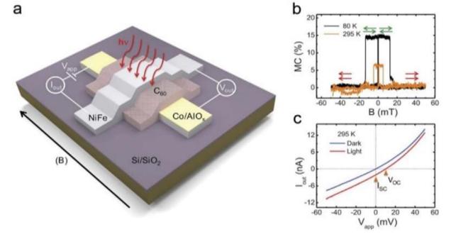
图4 (a) C60基分子自旋光伏器件示意图; (b) 暗场条件下的磁电流(10 mV偏压); (c) 室温下有/无白光辐照(7.5 mW/cm2)下的电流-电压曲线[45]

Fig.4 (a) Schematic representation of the C60-based molecular spin-photovoltaic device. (b) Magnetocurrent at a bias of 10 mV in dark conditions. (c) Current-voltage curves with and without white-light irradiation (7.5 mW/cm2) at room temperature

(4) Spin Field-Effect Transistor
Spin field-effect transistors were first proposed in 1990 by Das and Datta[46].The ferromagnetic source and drain electrodes have the same polarization direction (i.e., the orientation of electron spins is the same), enabling the injection and collection of spin-polarized electrons; the gate electric field causes the spins of high-speed electrons in the channel to precess or rotate. When the spin becomes antiparallel, it is repelled by the drain and does not conduct— the strength of this drain-repulsion effect depends on the degree of spin precession, thereby allowing the source–drain current to be controlled by the gate voltage. If a magnetic field is applied to the spin field-effect transistor, the conductivity's response to the magnetic field also exhibits an excellent magnetic switching effect. Studies have shown that the conductivity of a spin field-effect transistor exhibits distinct quantum oscillation effects as the thickness of the intermediate semiconductor layer and the magnetization directions of the ferromagnets on both sides vary, and factors such as the matching between the ferromagnetic and semiconductor valence bands also have a significant impact on conductivity (Figure 5) [47].
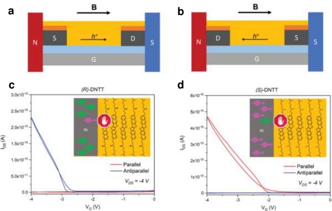
图5 (a)平行和(b)反平行磁场B条件下的铁磁电极的底栅底部接触(BGBC)OFET器件结构;c)平行(红色)和反平行(蓝色)磁场中(R)-DNPTT和(d)(S)-DTNTT在饱和状态(Vd = -4 V)下的迁移曲线[47]

Fig.5 Geometry of a BGBC (bottom-gate bottom-contact) OFET device with ferromagnetic electrodes (a) in a parallel and (b) in an antiparallel magnetic field (B). (c) Transfer curves in saturation regime (Vd = -4 V) of (R)-DNTT and (d) (S)-DNTT in a parallel (red) and antiparallel (blue) magnetic field

(5) Spin memristor
Memristors are the fourth fundamental circuit element, alongside resistors, capacitors, and inductors. They feature high speed, low power consumption, high integration density, and the dual functions of information storage and computation, making them regarded as the most promising future logic computing devices[48-49]. The structure of organic spin memristors and spin valves remains similar, primarily by integrating memristive properties with spin polarization effects. The basic structure of a spintronic memristor is a magnetic tunnel junction, where the spin-transfer torque effect and spin-orbit torque effect are used to modulate the influence of spin-polarized current on local magnetic moments, thereby altering the magnetization direction (Figure 6)[50]. By mimicking the brain's highly efficient and energy-saving operating mode, spin memristors can reduce the energy consumption of AI applications to 1/100th of that of conventional devices, while offering faster information processing speeds, higher information storage density, lower power consumption, and improved durability.
图6 自旋电子忆阻器器件结构示意图[50]

Fig.6 Schematic diagram of the spintronic memristors

3 Organic spintronic materials

Organic semiconductors are crystalline or amorphous materials composed of light elements such as carbon, hydrogen, oxygen, and nitrogen. Molecules stack in an ordered or disordered manner via weak van der Waals forces, resulting in relatively weak intersystem crossing and hyperfine coupling. These materials exhibit long spin relaxation times and relaxation distances, enabling effective spin control of charge carriers and full utilization of their spin properties. By fully leveraging the charge and spin degrees of freedom of charge carriers, organic semiconductors have emerged as ideal candidate materials for studying spin carrier transport[51-52]..
The conductivity of organic semiconductors arises from their π-conjugated structure, where the lower-energy π orbitals (the highest occupied molecular orbital, HOMO) resemble the valence band in inorganic materials, while the higher-energy π* orbitals (the lowest unoccupied molecular orbital, LUMO) resemble the conduction band, with a band gap of approximately 1.5–3.0 eV. Electrons can be delocalized within individual organic semiconductor molecules but cannot be delocalized throughout the entire organic semiconductor solid; therefore, charge transport in organic semiconductors primarily relies on intermolecular interactions rather than continuous energy bands. Organic semiconductors exhibit large exciton binding energies and long lifetimes, facilitating controllability and enabling multifunctional material design. However, charge mobilities are generally low, and the disordered molecular arrangement in organic materials increases carrier scattering, resulting in slow carrier transport and non-uniform performance. Even with long spin lifetimes, spin diffusion lengths remain limited. Moreover, the long spin lifetimes pose challenges for spin control, necessitating a combined approach that integrates interface engineering and the application of external electric, magnetic, or optical fields, starting from the intrinsic structural design of organic semiconductors. In addition, organic materials are susceptible to moisture, oxygen, and light, are not heat-resistant, and may degrade. Furthermore, energy level mismatches and interface defects between organic materials and metal electrodes can lead to low spin injection efficiency, thereby limiting the overall performance of organic spintronic devices[53]..

3.1 Magnetic and Nonmagnetic Organic Spin Materials

The spin-electronic effect in ferromagnetic materials arises from their unique electronic structure. In ferromagnetic metals or metal oxides, the exchange interaction of outer-shell electrons leads to differences in the densities of spin-up and spin-down electrons at the Fermi level, resulting in different electron currents for different spin orientations—i.e., spin currents. If the electronic structure or spin interactions in organic materials are similar to those in ferromagnetic metals, then a spin-electronic effect will likewise be observed[54].Several theoretical models can be used to explain the magnetism of organic materials, including: (1) the orthogonal intermolecular orbital model, in which, due to orbital orthogonality and a zero overlap integral, the exchange integral dominates; since the exchange integral is typically greater than zero, this leads to ferromagnetism; (2) the spin-polarization model, in which the imbalance between electrons in positive and negative spin states gives rise to magnetism in the material; (3) the intermolecular charge-transfer model, in which intermolecular charge transfer generates cationic radicals (D+) and anionic radicals (A-), and the D+A- biradical can exist in a triplet state with parallel spins and exhibit ferromagnetism; (4) the high-spin ground-state model, in which the parallel alignment of unpaired electrons within molecules results in a triplet ground state, thereby giving rise to magnetism; this model is often applicable to polymeric materials. Therefore, two fundamental principles guide the design of organic spin-electronic materials: (1) introducing paramagnetic centers (radicals) with unpaired electrons into the molecule; and (2) ensuring that neighboring paramagnetic spin centers have sufficiently strong interactions to generate a positive exchange integral[55].
In addition, non-magnetic organic semiconductor materials can also exhibit magnetic responses in current, electroluminescence, photoluminescence, and photocurrent under an external magnetic field, which is related to the field-dependent singlet/triplet exciton ratio. When the external magnetic field exceeds the spin-orbit coupling, the electron-hole separation distance determines whether the competition between the singlet-triplet energy difference and the Zeeman splitting via spin-exchange interactions can be harnessed to activate the magnetic field effect[56]. Currently, a variety of organic materials have been found to exhibit spintronic effects[3,57], including small-molecule materials—both metal-containing and purely organic—polymer materials, exciplexes, and even organic-inorganic hybrid materials such as perovskite materials. The design and development of organic spin semiconductors have entered a phase of diverse and flourishing innovation.

3.2 Organic small molecules

Organic small-molecule materials play a crucial role in the development of organic spin optoelectronic devices, including planar conjugated molecules, metal complexes, fullerenes and their derivatives. The earliest small-molecule materials used in organic spin devices were sexithienyl (T6) and aluminum 8-hydroxyquinolate (Alq₃)[58-59]. Subsequently, metal complexes based on 8-hydroxyquinoline[60-62], phthalocyanines (Pc) and their metal complexes, fullerenes and their derivatives, as well as other small-molecule materials, have been continuously developed[63-64] (Figure 7). In organic spin devices, the main advantage of organic small-molecule materials lies in the relative simplicity of device fabrication via thermal evaporation: the morphology of the intermediate layer can be controlled by adjusting the substrate temperature, both organic and metal layers can be deposited via evaporation without breaking the vacuum, and under ultra-high-vacuum evaporation, organic molecules grow in an amorphous form, enabling the formation of smooth organic thin-film surfaces.
图7 用于有机自旋器件的常见小分子材料

Fig.7 Typical small molecules for organic spin devices

(1) Metal complexes
Alq3is a representative organic spintronic material, characterized by its simple synthesis, easy purification, good film-forming properties, strong charge carrier transport capability, and high luminescence performance. In 2004, the giant magnetoresistance effect (GMR) was first observed in an LSMO (La2/3Sr1/3MnO3)/Alq3/Co spin-valve device, with a magnetoresistance ratio (MR) reaching 40%[58]. Barraud et al.[65]fabricated an LSMO/Alq3/Co magnetic tunnel junction at the nanoscale, achieving an MR as high as 300%. This significant enhancement in MR is attributed to the interface spin-related metal/organic molecule hybridization, which markedly strengthens the effective spin polarization. Recently, Yang et al.[66]used a thin film of (La2/3Pr1/3)5/8Ca3/8MnO3, which exhibits pronounced electronic phase separation, as an electrode based on Alq3, achieving an MR as high as 440%. In addition to Alq3, quinoline complexes with similar structures also exhibit excellent performance. Spin-valve devices fabricated using the novel lanthanide quinoline molecule NaDyClq allow for the control of electron spin through the chemical diversity of the molecule; the alternating NiFe and Co electrodes in direct contact with the NaDyClq film can modulate the switching of the device's magnetoresistance (MR) signal[67]. Alq3, Gaq3, and Inq3all possess spin-polarized interfacial states, and the three quinoline complexes exhibit virtually no difference in their interfacial properties, with coordination metal ions having minimal influence. These materials share the advantages of Alq3, including ease of synthesis, simple purification, and good film-forming properties. Recently, Hsu et al.[68]incorporated paramagnetic Fe into a quinoline complex to synthesize Feq3and found that electrons can be transferred from Co to Feq3, reducing Fe3+to Fe2+and generating spin polarization at the Co/Feq3interface. Consequently, after Fe2+comes into contact with ferromagnetic Co, it also exhibits ferromagnetic behavior. Thus, redox reactions at the metal/organic interface are not only the primary cause of spin polarization but also a key factor in the fabrication of spin-optoelectronic devices.
Unlike Alq3-type complexes, phthalocyanines (Pc) and their metal complexes can self-assemble on substrate surfaces to form well-organized structures, and their electronic properties and interfaces can be tuned by varying the metal surface and central ion. Different central coordinating ions, including Cu2+, Co2+, and Fe2+, enable metal phthalocyanine molecules to chemisorb onto Co surfaces, forming hybridized interfacial states that can be further modulated by different chemisorbed molecules, thereby enabling more diverse spin-selective injection[69].
Barraud et al.[70]fabricated nanoscale Co/CoPc/Co magnetic tunnel junctions and observed a negative tunneling magnetoresistance effect (Figure 8),which arises from different coupling lengths at the top and bottom of the Co/CoPc interface, leading to opposite spin polarization. Sun et al.[71]investigated the MR performance of fluorinated CuPc (F16CuPc) in a Co/AlO x/F16CuPc/NiFe structure. Smooth amorphous F16CuPc films prepared using low-temperature deposition techniques exhibit a spin diffusion length of up to 180 nm and an MR exceeding 4% at 295 K. Terbium bisphthalocyanine complex (Tb[PcPO3Et2]2) forms conjugate bonds with the LSMO surface, displaying strong hybridization effects, and its MR properties differ significantly across different temperature ranges (above or below 50 K).
图8 酞菁钴的隧道磁电阻效应。(a)Co/CoPc/Co磁性隧道结纳米接触示意图;(b)2 K温度下的I-V曲线;(c, d)在0°和180°时的磁阻曲线[70]

Fig.8 Tunneling magnetoresistance effect of Cobalt phthalocya-nine. (a) Magnetic tunnel junction contact for Co/CoPc/Co; (b) I-V curve at 2 K; (c, d) R (H) curves at 0° and 180°

(2) Fullerenes, Graphene, and Their Derivatives
Non-metallic organic compounds can also exhibit spin transport properties, with fullerenes being the most important and extensively studied[72]. Fullerenes possess excellent mechanical strength and can resist metal diffusion during the deposition of metal electrodes. With a 12C nuclear content of up to 99%, fullerenes lack nuclear spin, and thus exhibit no hyperfine interactions, resulting in relatively simple spin transport and long spin relaxation times[73-74]. C60in fullerenes was among the first materials studied in spintronics, exhibiting a spin transport length of up to 110 nm at room temperature. Subsequently, Liang et al.[75]found that C70films display a longer spin diffusion length than C60films, owing to different orbital electron hybridization at the Co/fullerene interface, which leads to distinct spin polarization. Zhang et al.[76]attribute this to the lower symmetry of C70, which results in greater spin scattering. In addition, two-dimensional (2D) ferromagnets also hold remarkable potential in emerging concepts of spintronics; it is generally believed that the Curie temperatures of most reported intrinsic 2D ferromagnets are well below room temperature. Furthermore, it has been found that adsorbing C60molecules onto the CoO surface leads to charge redistribution, thereby altering the electronic occupancy of the Co atom’s dorbitals and the O atom’s porbitals, which in turn enhances the antiferromagnetic coupling of Co atoms in CoO and the stability of its magnetism[77]. Recently, Lv et al.[78]used surface synthesis and solid-phase reactions to prepare, through atomic-level control, magnetically asymmetric graphene nanoribbons. The asymmetric sawtooth edges of these ribbons break the material’s spin symmetry, giving rise to unique ferromagnetic edge states and yielding the world’s first one-dimensional ferromagnetic carbon chain, thereby providing a new pathway for assembling a new generation of robust spin arrays.
(3) Large conjugated molecules
Research on the spin properties of molecules with large conjugated planar structures has been a focus of attention in recent years[47].Tajima et al.[79]synthesized a compound with high semiconductor performance based on a quinoid benzodithiophene structure. The diode devices made from this molecule exhibited significant current variations in magnetic fields below 100 mT and showed a strong dependence on measurement temperature. Furthermore, as the number of triplet biradicals increased at higher temperatures, the magnetoresistance (MR) value rose, reaching -19.4% at 120 ℃—the largest negative MR ever reported for an organic molecule—demonstrating a strong correlation between MR and the concentration of triplet biradicals. Ding Shuaishuai et al.[40]fabricated an organic single-crystal spin valve using large-area thin-film single crystals of pentacene derivatives, achieving a magnetoresistance as high as 17% and observing spin transport even in single crystals up to 457 nm thick.
Recently, Ma Yuguang’s team[80]exploited the high electron affinity of perylene diimide (PDI) molecules to obtain PDI anion solutions via ionization. By controlling the molecular self-assembly process, they formed densely packed PDI crystals. Subsequently, they discovered that a spontaneous oxidation process generated metastable high-density radicals, leading to the observation of room-temperature ferromagnetism in PDI radical crystals. The Curie temperature exceeds 400 K, and the saturation magnetization at room temperature reaches 1.2 emu/g. Meanwhile, the material exhibits typical n-type semiconductor properties, with a Hall mobility at room temperature of 0.5 cm2·V-1·s-1, displaying characteristic ferromagnetic features. This marks the first time room-temperature ferromagnetism has been observed in an organic semiconductor (Figure 9). Hu Wenping et al.[81]used a simple solution-based method to construct radical-doped organic cocrystals. The resulting fluorene-7,7,8,8-tetracyanoquinodimethane organic cocrystal radicals exhibit enhanced ferromagnetism and conductivity due to the strengthened charge-transfer interactions induced by the radicals, with a coercive field of 96 Oe and a Curie temperature close to 400 K.
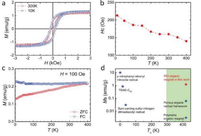
图9 PDI在(a)10和300 K温度下PDI粉末的M-H磁滞回线;(b)矫顽磁场的温度依赖性;(c)外加磁场下随温度变化的磁化曲线;(d)不同温度下纯有机磁体的饱和磁化性质[80]

Fig.9 Magnetic properties of PDI powder. (a) M-H hysteresis loops taken at 10 and 300 K. (b) Temperature dependence of the coercive field. (c) Magnetization measured at an applied magnetic field of 100 Oe at different temperatures. (d) Saturated magnetization versus Tc of the purely organic magnets

(4) Chiral optoelectronic molecules
Since the orbital angular momentum of non-chiral organic materials is almost negligible, chiral photoelectric molecules that exhibit both chirality and ferromagnetism are particularly important for expanding the spintronics applications of chiral materials and uncovering additional physical properties of chiral materials due to their coupling between spin and chiral light, as well as the simultaneous breaking of spatial and temporal symmetry[82-83]. The process by which organic chiral molecules induce spin selection primarily relies on tunneling mechanisms, which are particularly pronounced in short-range molecular junctions or monolayer structures; under certain conditions, such as in relatively thick or disordered systems, hopping transport may also play an auxiliary role, thereby weakening spin selectivity; band transport, however, plays virtually no role in organic chiral materials. Qin Wei et al.[84]reported a pair of organic chiral antiferromagnetic enantiomers, where molecular torsion arising from the propeller-like arrangement of donor and acceptor molecules gives rise to chirality, and differences in electron–phonon coupling between donors and acceptors in the chiral crystal give rise to antiferromagnetism. Because spin polarization is strongly dependent on chirality, at 10 K the magnetization of the right-handed antiferromagnetic crystal is 300% greater than that of the left-handed crystal; excitation and recombination processes are closely linked to spin, phonons, and chiral orbitals in these chiral antiferromagnets, greatly enriching the content of organic spintronics research and material design approaches (Figure 10). Subsequently, they found that the energy difference between the singlet and triplet states in thermally activated delayed fluorescence (TADF) chiral enantiomers increases with the strength of chirality, and that the elimination of spin degeneracy induced by chiral orbitals can enhance spin relaxation, while circularly polarized luminescence (CPL) is enhanced under the influence of an external magnetic field[85].
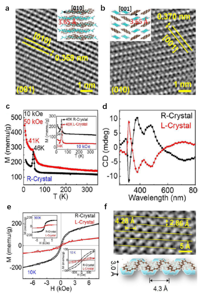
图10 (a, b) 高分辨电镜和单晶衍射; (c) 不同外加磁场下磁化强度的温度依赖性曲线; (d) 圆二色性; (e)10 K温度下磁滞曲线和(f)共晶螺旋分子排布的高分辨电镜[84]

Fig.10 (a, b) HRTEM of Bper-FTCNQ crystals and single-crystal X-ray diffraction; (c) temperature dependence of magnetization with different applied magnetic fields; (d) opposite circular dichroism signals and (e) M-H loops of R-Crystal and L-Crystal at 10 K; (f) spiral molecular arrangement of HRTEM inside the cocrystal

Crivillers et al.[86]prepared slurry-form perchlorotriphenylmethyl radicals with one (mPTM) or two (bPTM) terminal phenylethynyl groups. The phenylethynyl groups can react with gold, thereby grafting mPTM and bPTM onto the gold surface. Although mPTM and bPTM exhibit chirality and paramagnetic properties, no chiral-induced spin phenomenon was observed, possibly because their racemization energy barrier (22 kcal/mol) is relatively low. Kim et al.[87]used chiral amine organic ligands to synthesize chiral metal halide semiconductors and found that these materials grow along the out-of-plane direction during spin-coating, resulting in a highly c-axis-oriented and highly crystalline structure. Consequently, they achieved a strong chiral-induced spin effect, with MR values of 43% and 41% for R- and S-type metal halide semiconductors, respectively. In 2023, Yamamoto et al.[88]observed both an effective enhancement of spin–orbit interactions and a pair of oppositely polarized spins simultaneously during magnetoresistance measurements near the superconducting transition temperature in organic chiral superconductors. The spin polarization obtained was several orders of magnitude higher than that induced by the Edelstein effect, indicating that spin–orbit interactions were effectively enhanced, which is associated with the antiparallel spin polarization at the two ends of chiral molecules. Electron–chirality interactions significantly influence charge and spin transport in chiral conductors. Narcis et al.[89]successfully fabricated combined magnetic diode and spin-valve devices based on helicene single-molecule junctions. The magnetic diode behavior can be attributed to the interaction between the angular momentum of electrons in the chiral medium and the magnetic field, while the spin-valve function arises from the interaction between electron spin and the chiral medium. The coexistence of these electron–chirality interactions at the atomic scale and their functional integration further expand the scope of research in spintronics.
(5) Organic Radicals
Organic radicals exhibit rich spin-flip and luminescence behaviors and have recently stood out in fields such as OLEDs[90-91].At the same time, open-shell molecules containing stable radicals, with their unpaired electrons, also display unique magnetic response behaviors. Due to their weak spin–orbit coupling and hyperfine interactions, they constitute an important class of organic spintronic materials[92-93].Boudouris et al.[94]combined non-conjugated 2,2,6,6-tetramethylpiperidine-1-oxyl (TEMPO) with a liquid-crystalline structure to prepare TEMPO-based stable radical derivatives. They found that under crystalline conditions, these derivatives exhibit a conductivity of up to ~15.6 S·m-1 at room temperature, and at 10 K, a 100% MR value was observed under a 2 T magnetic field. Single-crystal analysis revealed a short inter-radical distance of only 6.1 Å, which contributes to their high macroscopic electrical conductivity and magnetic field responsiveness.Amorphous, non-conjugated free-radical polymers with main-chain–side-chain interactions and low glass-transition temperatures enable rapid charge transport in the solid state due to strong coupling between the main chain and side chains, with conductivities exceeding 32 S·m-1. On a 1.5 μm-thick film, these polymers can maintain 98% optical transparency[95].Casu et al.[96]deposited a monolayer of pyrene-derived radical molecules on a polycrystalline Co surface and found that the electronic hybridization between the organic molecules and the metal atoms can influence the electronic structure of Co, leading to a reduction in the magnetic moment of Co atoms and the loss of radical character in the organic molecules. This suggests that designing radical molecules capable of adsorbing onto the surface of ferroelectric materials could be an important approach for constructing spintronic materials. Mannini et al.[97]prepared chiral molecular radicals (ESAc, see Fig. 7) and deposited them as a monolayer on a gold surface. EPR measurements detected a paramagnetic signal (Fig. 11), and the fabricated devices exhibited chiral-induced spin selectivity. Magnetic conductive atomic force microscopy revealed an MR value of 60% at room temperature, marking the first observation of a chiral-induced spin effect in organic radicals.
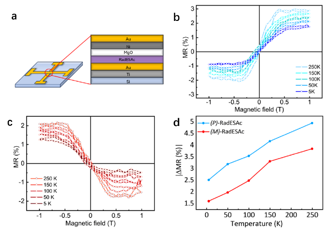
图11 (a) 磁阻器件的结构示意图; (b, c) (P)-RadESAc@Au和(M)-RadESAc@Au单分子层的磁阻百分比;(d) 两种对映体的磁阻差异值温度依赖关系[97]

Fig.11 (a) Scheme of the magnetoresistance device with magnification on the cross junction. Magnetoresistance percentage of (b) (P)-RadESAc@Au and of (c) (M)-RadESAc@Au monolayers. (d) |ΔMR (%)| values as a function of the temperature for both the enantiomers

(6) Other small molecules
Currently, there are many metal-free organic spin materials, such as Rubrene. Rubrene boasts high carrier mobility and good chemical stability; the first all-organic spin-valve device was based on Rubrene[98]. Recently, Zhang et al.[76]used Fe3O4 as a ferromagnetic electrode and found that the MR of Rubrene reaches 6% at room temperature; Li et al. used spin-pump devices to study spin transport in Rubrene, obtaining a spin transport length of 132 nm and a spin lifetime of 3.8 ms[99]. Similar to Rubrene, Bathocuproine has also attracted considerable attention, as it exhibits excellent air stability, mechanical ductility, and room-temperature spin transport properties[71,100]. In addition, 6,13-bis(triisopropylsilylethynyl)pentacene exhibits a spin diffusion length of 24 nm[101].
Gallego et al.[102]theoretically investigated electron transport in ditolyl under external magnetic field conditions, predicting an MR value of approximately -0.07% at 1.1 V. Zhang Chuang et al. prepared rubrene microcrystals using a capillary bridge assembly method (Figure 12),whose photoluminescence decreased by >40% in a 10 mT magnetic field. This is because, under a magnetic field, luminescence depends on singlet–triplet conversion involving triplet–triplet pairs, and the singlet fission and triplet fusion processes in the radiative decay exhibit significant magnetic field dependence[103].Furthermore, the size of the microcrystals is crucial for magneto-optical effects, as it influences the photophysical processes of spin-state transitions. Consequently, magneto-optical effects can be tuned by controlling microcrystal size, enabling the design of chip-scale optomagnetic sensors that exploit exceptional low-field sensitivity across a broad frequency range (from Hz to MHz) to detect magnetic field strength, thereby demonstrating a class of emerging photospintronics molecular prototype devices.
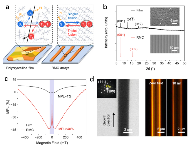
图12 红荧烯的巨磁阻发光性质(MPL): (a) 红荧烯薄膜和微晶的自旋反转; (b) 红荧烯薄膜的X射线衍射和(c) MPL;(d) 单个微晶的透射电子显微镜和光学成像[102]

Fig.12 Observation of giant MPL in RMCs. (a) Illustration for the spin conversion and (b) X-ray diffraction patterns and (c) typical MPL(B) curves of rubrene film. (d) Transmission electron microscopy image and optical images of a single RMC

3.3 Polymer Materials

Organic spintronic devices can also use polymer materials[104-105].Compared with organic small-molecule materials, polymers offer advantages such as ease of solution processing, low-cost fabrication, and high flexibility (Figure 13). Polymer spin materials can be classified into three categories: conjugated polymers, coordination polymers, and ferroelectric polymers.
图13 用于有机自旋器件的常见聚合物材料

Fig.13 Typical polymers for organic spin devices

(1) Conjugated polymers
Many conjugated polymers with different conjugated units can be used in organic spintronic devices. These conjugated units include thiophene[106-107],phenylene vinylene[108],naphthalenediimide (NDI)[109-110],pyrrolopyrrole dione (DPP)[111],isoindigo (IID)[112], and others. Take P3HT as an example: P3HT is widely used in organic photovoltaic devices (OPVs). To address the penetration issue during the deposition of metal electrodes, Ding et al.[113] developed a sacrificial layer transfer technique to tailor the spin interface between organic semiconductors and ferromagnetic electrodes, thereby obtaining a well-defined interface between metal electrodes and organic materials, which exhibits a significant and stable MR effect. Building on this, they also fabricated a La2/3Sr1/3MnO3/P3HT/Co spin valve, achieving an MR value as high as 93%[114]. Geng et al.[106] used the P3HT system to investigate the impact of charge distribution on hyperfine coupling. In single-hole devices of ITO/PEDOT/P3HT/Au, they found that as the annealing temperature increased and the crystallinity of P3HT improved, hyperfine coupling weakened, while the spin diffusion length increased. Based on P3HT, Shen Baogen et al.[41] combined strain electronics with organic spintronics to construct, for the first time, a polymer spin valve device with a gate structure. By leveraging the unique spin interface effects in organic/inorganic systems, they achieved a magnetoresistance as high as 281% and, through in-situ control via gate voltage, created 10 stable operating states within a single device, significantly increasing the storage density of conventional spin valve devices.
NDI-based D-A copolymers are widely used in OPVs and organic field-effect transistors (OFETs)[115-116],with a low LUMO energy level and excellent electron-transport properties. Zhang et al.[110]fabricated the first spin-valve device based on the NDI copolymer P(NDI2OD-T2), achieving an MR value of 90% at 4.2 K and 6.8% at 300 K, indicating the great potential of D-A copolymers in organic spintronic devices. Also based on NDI acceptor units, Yu et al.[109]prepared a series of D-A copolymers, including PNVT-CN-8, which exhibit stable MR effects at room temperature. It was found that extending the alkyl chains or substituting with cyano groups reduces the MR effect; NiFe/Au/PNVT-CN-8/Co shows a negative MR effect, while the MR value increases when the bottom ferromagnetic electrode is changed from NiFe to LSMO. DPP-based D-A copolymers are also extensively used in organic spintronic devices[117-118],and by selecting and optimizing the donor and acceptor types and their ratios, p-type, n-type, or bipolar charge transport can be achieved. Yu et al.[110]used DPP units to prepare a series of PTDCNTVT conjugated polymers with different alkyl chains; in the PTDCNTVT-420/Co/Au device, longer alkyl chains exhibited a higher MR effect (up to 30%), and the choice of top electrodes Co or NiFe also had a significant impact on the MR effect, with devices based on NiFe electrodes showing higher MR values. Similarly, conjugated polymers based on IID units have also developed rapidly, exhibiting outstanding field-effect and photovoltaic performance. Li et al.[111]prepared four D-A conjugated copolymers using IID and azaindigo (AIID), and found that introducing pyridine N alters the electronic structure and enhances the MR effect; introducing differently branched alkyl chains changes the aggregation structure, and the MR effect decreases as the alkyl chains are extended. Many conjugated polymers with different conjugated units can be used in organic spintronic devices, including thiophene[106,119],phenylene vinylene[108],naphthalenediimide (NDI)[109-110],pyrrolopyrrole dione (DPP)[111],and isoindigo (IID)[113], among others.
(2) Coordination polymers
Coordination polymers are inorganic or organometallic polymers containing linked metal cation center structures, and are coordination compounds with repeating coordination entities that extend in three dimensions. Therefore, while conjugated polymers possess only a one-dimensional conjugated backbone structure, coordination polymers can exhibit two- or even three-dimensional conjugated structures. Well-known coordination polymers, such as metal–organic framework materials (MOFs), contain both metal ions/clusters and organic linker units; early MOFs had low electrical conductivity and were essentially insulating[120]. Recently developed MOFs, however, have exhibited semiconductor properties[121-122]. In MOFs, the organic linker units facilitate spin transport, while metal ions with high spin–orbit coupling (SOC) can modulate spin states; numerous review articles have been published on this topic[123]. Song et al.[124]were among the earliest to explore MOF-based spintronic devices, preparing highly crystalline and oriented conjugated MOF thin films of two-dimensional hexahydroxytriphenylene copper Cu3(HHTP)2via layer-by-layer assembly. By using these films as an organic interlayer, they found that the spin-valve magnetoresistance (MR) could reach as high as 25% at 10 K (Fig. 14), and that the films maintained good thickness adaptability within a thickness range of 30–100 nm and under high-temperature conditions up to 200 K. Academician Xinliang Feng and colleagues introduced bulky side groups onto the conjugated ligands, causing a significant shift in the stacking mode of two-dimensional conjugated metal–organic frameworks (2D c-MOFs) from zigzag stacking to staggered stacking, thereby spatially weakening the interlayer interactions. As a result, the electrical conductivity of 2D c-MOFs decreased by six orders of magnitude, while the spin density increased by more than 30-fold and the spin–lattice relaxation time increased by 60 μs[125-126].
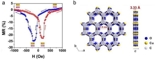
图14 (a) LSMO/Cu3(HHTP)2/Co 有机自旋阀在10 K下的MR循环;(b) Cu3(HHTP)2的俯视图和侧视图[124]

Fig.14 (a) The MR loop for the LSMO/Cu3(HHTP)2 (100 nm)/Co organic spin valves at 10 K; (b) the top and side view of Cu3(HHTP)2 (proposed space filling drawings in slipped-parallel stacking mode, Hydrogen atoms are omitted for clarity)

Two-dimensional conjugated organic frameworks (2D COFs) are crystalline, layered, organic porous materials with excellent structural tunability and represent another class of typical coordination polymers. Cortes et al.[127]conducted a systematic theoretical study on 2D COFs containing conjugated rings such as benzene, borazine, and triazine, and found that the incorporation of transition metals—both the amount and the specific sites of incorporation—can significantly alter the electronic properties, magnetic behavior, and spin characteristics of 2D COFs. Yang et al.[128]theoretically designed two-dimensional graphene-based organic hybrid (COFs/MOFs) quantum dot materials with ferromagnetic properties at room temperature, suggesting that the Curie temperature of this two-dimensional magnetic semiconductor material can be raised to 472 K. They proposed the possibility of designing two-dimensional ferromagnetic materials based on TZGDs, thereby advancing research on two-dimensional ferromagnetic materials in the contexts of magnetic quantum dots and molecular magnets. Graphene, as a two-dimensional (2D) layered material, consists of a single-atom-thick hexagonal network of sp 2-hybridized carbon atoms, exhibiting high intrinsic carrier mobility and thermal conductivity, a relatively long spin diffusion length, weak intrinsic spin-orbit coupling, and limited hyperfine interactions; it is therefore also regarded as a highly promising material for next-generation spintronic applications. Yan Wensheng et al.[129]achieved strong room-temperature ferromagnetism in graphene by embedding isolated Co atoms via coordinated N atoms, where orbital hybridization among cobalt, nitrogen, and carbon gives rise to ferromagnetic exchange interactions, resulting in a TC as high as 400 K and a saturation magnetization of 0.11 emu·g-1 (at 300 K).
(3) Ferroelectric polymers
Ferroelectric materials are those that exhibit spontaneous polarization within a certain temperature range, and whose polarization direction can be reversed by an external electric field[130-131]. Ferroelectric polymers are polymeric materials that possess ferroelectric properties[83]. In ferroelectric polymers, dipoles align in a unidirectional, ordered manner to form ferroelectric domains with spontaneous polarization, exhibiting excellent dielectric constants and dielectric strengths, making them an ideal choice for developing high-energy-density thin-film dielectric materials. Currently reported ferroelectric polymers include polyvinylidene fluoride (PVDF), vinylidene trifluoride copolymer P(VDF-TrFE), odd-numbered nylon, and polyurea. Among these, PVDF and its copolymer P(VDF-TrFE) have been the most extensively studied[132-133]. Lu et al.[35]successfully integrated the tunneling magnetoresistance (TMR) effect into a memristor using PVDF. The La0.6Sr0.4MnO3 (LSMO)/PVDF/Co memristor with a thin organic barrier exhibits an extraordinary TMR of -266%. It was found that voltage-driven fluorine motion at the junction can induce a reversible resistivity change as large as 106% on a nanosecond timescale, and removing fluorine from the PVDF layer can suppress the dipole field in the tunneling barrier, thereby significantly enhancing TMR. Furthermore, due to the dramatic change in spin polarization at the LSMO/PVDF interface after F doping, the TMR can be tuned by applying different polarization voltages. The combination of TMR with organic memristors paves the way for developing high-performance multifunctional devices for storage and neuromorphic applications[134].

3.4 Excited-state complex

Exciplex complexes are aggregates of two different types of molecules, where strong intermolecular interactions lead to intermolecular charge transfer, resulting in new energy levels that provide abundant channels for spin flipping. By using ferromagnetic electrodes, spin devices based on exciplex complexes can be constructed. Exciplex complexes with a donor-acceptor structure facilitate the development of thermally activated delayed fluorescence materials with a very small singlet-triplet energy gap. In such materials, triplet emission can be efficiently utilized through reverse intersystem crossing, leading to excellent performance in conventional OLED devices. Moreover, their electroluminescence can be modulated by magnetic fields, enabling the fabrication of spin OLED devices. Professor Pang Zhiyong and colleagues prepared TADF exciplex-based spin OLED devices using m-MTDATA as the donor and 3TPYMB as the acceptor, and observed magnetoresponsive electroluminescence under various voltages and temperatures[135].Ma Dongge and colleagues[136]employed two types of exciplex complexes with different magnetic response behaviors in a single organic device. Under a fixed bias voltage and without the need for any ferromagnetic electrodes, they achieved tunable room-temperature magnetic conductivity. In the dark, the hyperfine coupling effect of ground-state charge-transfer complexes dominates, resulting in negative magnetic conductivity; under illumination, excited-state charge-transfer complexes dominate, leading to positive magnetic conductivity. As a result, exceptionally high magnetic conductivity was obtained near the turn-on voltage. Wang Kai and colleagues[137]found that certain non-fullerene bulk heterojunction systems, such as PM6:Y6 and PM6:IT-4F, exhibit significant in-plane and out-of-plane anisotropic magnetoresistance effects. The magnetoresistance ratio shows a clear two-fold symmetry as the magnetic field is rotated through 180°. They discovered that the magnetic response and magnetic anisotropy are determined by the anisotropic Landé g-factor difference and hyperfine coupling effects of polaron pairs in the organic donor-acceptor charge-transfer states.

3.5 Organic-inorganic hybrid materials

Organic materials, due to their light-element composition, weak SOC, and low hyperfine coupling, can maintain pure spin circuits or spin-polarized circuits, giving them an advantage in spin transport. However, strong SOC is indispensable for spin information processing and spin control, where inorganic materials excel. Consequently, organic-inorganic hybrid materials that combine the advantages of both types of materials have emerged[138-139]. Organic-inorganic hybrid materials exhibit significant Rashba splitting and magnetic field effects, possess strong SOC, and also feature relatively long spin lifetimes; these aspects have been summarized in several review papers[4,57,140]. Wang et al.[141]found that electroluminescence in LSMO/MAPbBr3/TPBi/Al devices (where MA denotes methylammonium) can be easily modulated by an external magnetic field (Fig. 15), and that LSMO/MAPbBr3/Co devices exhibit a pronounced GMR effect with an MR value exceeding 25% and a spin lifetime of approximately 936 ps. They also prepared MAPbBr3, MAPbI3, and FAPbBr3(FA denotes formamidinium) by varying the organic cation and halogen atoms; the performance of the resulting spin-valve devices indicates that halogen atoms have a stronger influence on the GMR effect than organic cations[142]. Yang et al.[143]fabricated a spin-pumping device with a Ni80Fe20/CH3NH3PbCl3- xI x/Pt structure, observing a spin diffusion length of approximately 61 nm at room temperature and finding that different compositions correspond to different spin relaxation mechanisms: iodine-based systems follow the EY mechanism, while bromine-based systems follow the DP mechanism. Li et al.[144]observed an MR as high as 97% and a spin diffusion length of up to 81 nm at 10 K in LSMO/MAPbI3/Co spin-valve devices. More interestingly, when the polycrystalline MAPbI3thin film was replaced with a single-crystal film, the spin diffusion length reached 1 μm at low temperatures. Wang Kai et al.[146]have conducted extensive research on perovskite-based spin-optoelectronic materials and devices, carrying out a series of studies on spin quantum tunneling and spin valves at the ferromagnet–perovskite spin interface[145], and they were the first to report the magneto-optical electroluminescence effect in quasi-two-dimensional chiral organic–inorganic hybrid perovskites.
图15 (a) 有机无机杂化材料的自旋阀器件及(b) 在10 K和0.1 V偏置电压下的GMR响应[141]

Fig.15 (a) Spin valve of organic-inorganic hybrid material and (b) the GMR response at 10 K and 0.1 V bias voltage

Two-dimensional organic-inorganic hybrid perovskites (2D HOIPs) can form multiple quantum wells, and their unique physical properties and potential applications in optoelectronic devices have attracted increasing research interest[138,142-144].Recent studies have shown that by incorporating chiral organic ligands into the organic layers, 2D HOIPs can exhibit spin-related characteristics. Vardeny et al.[147]reported spin-dependent photovoltaic and photocurrent responses in optoelectronic devices based on chiral 2D HOIPs. Under left- and right-circularly polarized light (CPL) excitation, the photocurrent difference between (R-MBA)2PbI4 and (S-MBA)2PbI4 was 10%, demonstrating selective spin transport through chiral multilayer films (Figure 16). They further doped benzyl viologen as an n-type material into 2D HOIPs, achieving a tunable Fermi level and higher electrical conductivity, with a Rashba splitting of 38 ± 4 meV and an electron spin g-factor of 6%[148]. Sun et al.[149]were the first to observe chiral phonon-driven spin currents in a two-dimensional layered organic-inorganic hybrid perovskite system with chiral cations. The introduction of chiral organic cations breaks the material’s spatial inversion symmetry, lifting the degeneracy of left- and right-circularly polarized phonon modes even in the absence of an external magnetic field, thereby resulting in non-zero phonon angular momentum. The measured spin Seebeck effect was approximately 104 A/(Km), which is even more significant. Organic-inorganic hybrid materials are widely recognized for their roles in both spin transport and spin control, and they are likely to receive greater attention and find improved applications in the field of organic spintronics in the future.
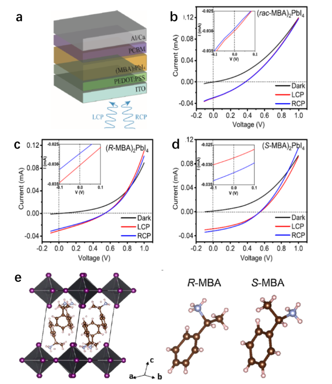
图16 (a) 自旋光伏器件示意图;(b) (rac-MBA)2PbI4, (c) (R-MBA)2PbI4和(d) 7 K条件下(S-MBA)2PbI4I-V响应;(e) 手性2D杂化钙钛矿(R/S-MBA)2PbI4的晶体结构[147]

Fig.16 (a) Schematic view of the spin photovoltaic device, the I-V response of the photovoltaic devices based on (b) (rac-MBA)2PbI4, (c) (R-MBA)2PbI4, and (d) (S-MBA)2PbI4 measured at 7 K. (e) Crystalline structure of (R/S-MBA)2PbI4[147]

4 Conclusion and Outlook

As an emerging discipline, organic spintronics is thriving, with rapid advancements in both material development and innovative applications in functional devices. A wide range of organic small molecules, conjugated polymers, and even emerging organic-inorganic hybrid materials are continuously being discovered and applied in various spintronic devices. The high degree of designability and tunability of organic molecules provides a unique advantage in realizing specific functions in spintronic devices. Rational design and modification of molecular structures significantly enhance charge carrier injection and transport in materials, particularly in terms of spin injection and spin-polarized current transport at interface layers. In-depth studies of molecular structures and their aggregation states will further deepen our understanding of spin injection and transport properties, thereby providing a foundation for developing the next generation of organic spintronic materials. However, organic spintronics is still in its early stages, and there is an urgent need to accumulate extensive experimental data, identify empirical patterns, and refine the theoretical foundations of organic semiconductor spintronics. Only with a sound theoretical framework can the structures of organic semiconductor materials and devices be optimized, allowing for better exploitation of the advantages of organic semiconductors in spintronics applications. These include: (1) refining theory by developing more precise spin transport models to guide material optimization; (2) advancing interface engineering, as spin injection efficiency is significantly influenced by interfacial hybridization, necessitating the development of novel interface modification strategies; (3) leveraging single-crystal devices, where the long-range ordered structure of organic single crystals can substantially enhance spin diffusion length and device performance; and (4) fostering multidisciplinary integration, as the convergence of chiral chemistry, radical materials, and quantum computing will open up new application domains.
In organic spin materials, chirality-mediated spin selectivity has emerged as an important aspect of spin interface control, and the intersection of organic chiral chemistry and spintronics holds promise for opening a new avenue for organic spintronics. Stable radical organic optoelectronic materials with paramagnetic properties possess unique advantages in spin devices and may represent an important direction for the future development of organic spin materials. Furthermore, examining the applications of organic spintronic devices, such as spin valves, the vast majority of research has focused on polycrystalline organic thin films. The polycrystalline structure of these films often contains numerous defects, resulting in low carrier mobility, which is detrimental to achieving long spin diffusion lengths. Moreover, the film structure is highly susceptible to preparation conditions. In contrast, organic single crystals feature long-range ordered structures and high carrier mobilities. Combined with the advantage of long spin relaxation times in organic materials, they hold great potential for achieving long spin diffusion lengths and for fabricating high-performance organic spintronic devices, which are expected to play an important role in the future of electronics.
[1]
Baibich M N, Broto J M, Fert A, Van Dau F N, Petroff F, Etienne P, Creuzet G, Friederich A, Chazelas J. Phys. Rev. Lett., 1988, 61(21): 2472.

[2]
Grünberg P, Schreiber R, Pang Y, Brodsky M B, Sowers H. Phys. Rev. Lett., 1986, 57(19): 2442.

[3]
Guo L D, Hu S H, Gu X R, Zhang R, Wang K, Yan W J, Sun X N. Adv. Mater., 2024, 36(22): 2301854.

[4]
Zakrzewski J J, Liberka M, Wang J H, Chorazy S, Ohkoshi S I. Chem. Rev., 2024, 124(9): 5930.

[5]
Kong D, Zhu C, Zhao C, Liu J, Wang P, Huang X, Zheng S, Zheng D, Liu R, Zhou J. Chem. Soc. Rev., 2024, 53: 11228.

[6]
Guo L, Gu X, Zhang R, Wang K, Yan W, Sun X. Adv. Mater., 2024, 36(22): 2301854.

[7]
Han J H, Cheng R, Liu L Q, Ohno H, Fukami S. Nat. Mater., 2023, 22(6): 684.

[8]
Yin G, Wu J, Ye L X, Liu L X, Yu Y X, Min P, Yu Z Z, Zhang H B. Adv. Funct. Mater., 2025, 35(18): 2314425.

[9]
Sun Y, Meng F H, Lee C M, Soll A, Zhang H R, Ramesh R, Yao J, Sofer Z, Orenstein J. Nat. Phys., 2024, 20(5): 794.

[10]
Li Y, Zhang Z T, Liu C, Zheng D X, Fang B, Zhang C H, Chen A T, Ma Y C, Wang C M, Liu H L, Shen K, Manchon A, Xiao J Q, Qiu Z Q, Hu C M, Zhang X X. Nat. Commun., 2024, 15: 2234.

[11]
Jin W L, Yang C-Y, Pau R, Wang Q Q, Tekelenburg E K, Wu H-Y, Wu Z A, Jeong S Y, Pitzalis F, Liu T F, He Q, Li Q F, Huang J-D, Kroon R, Heeney M, Woo H Y, Mura A, Motta A, Facchetti A, Fahlman M, Loi M A, Fabiano S. Nature, 2024, 630(8015): 96.

[12]
Karmakar S, Mukhopadhyay M K, Sanyal M K. Phys. Rev. Materials, 2024, 8(2): 024601.

[13]
Zhao H N, Arneson C E, Fan D J, Forrest S R. Nature, 2024, 626(7998): 300.

[14]
Zhou W X, Fei Y Y, Zhang Y S, Miao X H, Jiang S D, Liu J Z. Nat. Commun., 2025, 16: 1006.

[15]
Lu Y, Zhang Y Y, Yang C Y, Revuelta S, Qi H Y, Huang C H, Jin W L, Li Z C, Vega-Mayoral V, Liu Y N, Huang X, Pohl D, Položij M, Zhou S Q, Cánovas E, Heine T, Fabiano S, Feng X L, Dong R H. Nat. Commun., 2022, 13: 7240.

[16]
Yang T T, Qin Y, Wu M, Gu X R, Meng K, Hu S H, Zhang C, Guo A K, Zheng R H, Zhang R, Guo L D, Sun X N. Adv. Mater., 2024, 36(49): 2410695.

[17]
Nikl M. Nat. Photon., 2024, 18(2): 109.

[18]
Tschirhart C L, Redekop E, Li L Z, Li T X, Jiang S W, Arp T, Sheekey O, Taniguchi T, Watanabe K, Huber M E, Mak K F, Shan J, Young A F. Nat. Phys., 2023, 19(6): 807.

[19]
Dainone P A, Prestes N F, Renucci P, Bouché A, Morassi M, Devaux X, Lindemann M, George J M, Jaffrès H, Lemaitre A, Xu B, Stoffel M, Chen T X, Lombez L, Lagarde D, Cong G W, Ma T Y, Pigeat P, Vergnat M, Rinnert H, Marie X, Han X F, Mangin S, Rojas-Sánchez J C, Wang J P, Beard M C, Gerhardt N C, Žutić I, Lu Y. Nature, 2024, 627(8005): 783.

[20]
Xing D. Physics, 2005, 34(5): 348.

[21]
Shi Y, Gan Y S, Chen Y Z, Wang Y B, Ghosh S, Kavokin A, Xiong Q H. Nat. Mater., 2025, 24(1): 56.

[22]
Borst M, Vree P H, Lowther A, Teepe A, Kurdi S, Bertelli I, Simon B G, Blanter Y M, van der Sar T. Science, 2023, 382(6669): 430.

[23]
Žutić I, Fabian J, Das Sarma S. Phys. Rev. B, 2001, 64(12): 121201.

[24]
Hesselink L, Orlov S S, Liu A, Akella A, Lande D, Neurgaonkar R R. Science, 1998, 282(5391): 1089.

[25]
Hatefi Y, Haavik A G, Griffiths D E. J. Biol. Chem., 1962, 237(5): 1676.

[26]
Bloom B P, Chen Z W, Lu H P, Waldeck D H. Natl. Sci. Rev., 2024, 11(9): nwae212.

[27]
Zhu Z G, Su G. Sci. China Phys. Mech. Astron., 2013, 56(1): 166.

[28]
Bandyopadhyay S. Phys. Rev. B, 2010, 81(15): 153202.

[29]
Puja D, Jitendra N R. Spintronics fundamentals and applications. Singapore: Springer, 2021.

[30]
Muñoz L, Pérez E, Viña L, Ploog K. Phys. Rev. B, 1995, 51(7): 4247.

[31]
Tackeuchi A, Kuroda T, Nishikawa S, OsamuWada O. Jpn. J. Appl. Phys., 1999, 38(8R): 4680.

[32]
Britton R S, Grevatt T, Malinowski A, Harley R T, Perozzo P, Cameron A R, Miller A. Appl. Phys. Lett., 1998, 73(15): 2140.

[33]
Wilamowski Z, Werpachowska A M. Mater. Sci.-Poland, 2006, 24(3): 803.

[34]
Shahri Naseri M. Spin, 2023, 13: 2350008.

[35]
Nuccio L, Willis M, Schulz L, Fratini S, Messina F, D’Amico M, Pratt F L, Lord J S, McKenzie I, Loth M, Purushothaman B, Anthony J, Heeney M, Wilson R M, Hernández I, Cannas M, Sedlak K, Kreouzis T, Gillin W P, Bernhard C, Drew A J. Phys. Rev. Lett., 2013, 110(21): 216602.

[36]
Nachawaty A, Chen T X, Ibrahim F, Wang Y C, Hao Y F, Dalla Francesca K, Tyagi P, Da Costa A, Ferri A, Liu C C, Li X G, Chshiev M, Migot S, Badie L, Jahjah W, Desfeux R, Le Breton J C, Schieffer P, Le Pottier A, Gries T, Devaux X, Lu Y. Adv. Mater., 2024, 36(33): 2401611.

[37]
Hautzinger M P, Pan X, Hayden S C, Ye J Y, Jiang Q, Wilson M J, Phillips A J, Dong Y F, Raulerson E K, Leahy I A, Jiang C-S, Blackburn J L, Luther J M, Lu Y, Jungjohann K, Vardeny Z V, Berry J J, Alberi K, Beard M C. Nature, 2024, 631(8020): 307.

[38]
Nadeem M, Wang X L. Adv. Mater., 2024, 36(33): 2402503.

[39]
Li J, Ding S S, Hu W P. Acta Phys. Sin., 2022, 71(6): 067201.

[40]
Wang Y, Yao J R, Ding S S, Guo S Y, Cui D P, Wang X Y, Yang S Y, Zhang L J, Tian X Z, Wu D, Jin C, Li R J, Hu W P. Sci. China Mater., 2021, 64(11): 2795.

[41]
Zhang C, Ding S S, Tian Y, Ke Y Z, Wang J T, Wang J, Hu F X, Hu W P, Shen B G. Adv. Mater., 2025, 37(4): 2416629.

[42]
Jeon S, Han K, Shin H, Kim K, Jeong J, Kim J. Adv. Opt. Mater., 2018, 6(8): 1701349.

[43]
Taniyama T, Wada eiji, Itoh M, Yamaguchi M. NPG Asia Mater., 2011, 3(7): 65.

[44]
Lee Y, Jeong J, Jung K, Lee J, Youn Y, Park S, Lee H, Yi Y. Sci. Rep., 2025, 15: 745.

[45]
Sun X N, Vélez S, Atxabal A, Bedoya-Pinto A, Parui S, Zhu X W, Llopis R, Casanova F, Hueso L E. Science, 2017, 357(6352): 677.

[46]
Das B, Datta S, Reifenberger R. Phys. Rev. B, 1990, 41(12): 8278.

[47]
Volpi M, Jouclas R, Liu J, Liu G F, Catalano L, McIntosh N, Bardini M, Gatsios C, Modesti F, Turetta N, Beljonne D, Cornil J, Kennedy A R, Koch N, Erk P, Samorì P, Schweicher G, Geerts Y H. Adv. Sci., 2023, 10(26): 2301914.

[48]
Grollier J, Querlioz D, Camsari K Y, Everschor-Sitte K, Fukami S, Stiles M D. Nat. Electron., 2020, 3(7): 360.

[49]
Zhang B W, Bai T, Han L, Che S N, Duan Y Y. Adv. Mater., 2024, 36(35): 2403142.

[50]
Qin J J, Sun B, Zhou G D, Guo T, Chen Y Z, Ke C, Mao S S, Chen X L, Shao J Y, Zhao Y. ACS Mater. Lett., 2023, 5(8): 2197.

[51]
Dediu V A, Hueso L E, Bergenti I, Taliani C. Nat. Mater., 2009, 8(9): 707.

[52]
Sanvito S. Nat. Phys., 2010, 6(8): 562.

[53]
Pope M, Swenberg C E. Electronic Processes in Organic Crystals and Polymers. 2nd ed. Oxford: Oxford University Press, 1999, 877.

[54]
Shi Y, Gan Y S, Chen Y Z, Wang Y B, Ghosh S, Kavokin A, Xiong Q H. Nat. Mater., 2025, 24(1): 56.

[55]
Coronado E. Nat. Rev. Mater., 2020, 5(2): 87.

[56]
Yan L, Wu Y, Xu Z H, Hu B. Synth. Met., 2009, 159(21/22): 2323.

[57]
Zhu Y N, Jiang Q L, Zhang J, Ma Y G. Chem., 2023, 18(3): e202201125.

[58]
Xiong Z H, Wu D, Valy Vardeny Z, Shi J. Nature, 2004, 427(6977): 821.

[59]
Jiang S W, Liu S, Wang P, Luan Z Z, Tao X D, Ding H F, Wu D. Phys. Rev. Lett., 2015, 115(8): 086601.

[60]
Bergenti I, Borgatti F, Calbucci M, Riminucci A, Cecchini R, Graziosi P, MacLaren D A, Giglia A, Rueff J P, Céolin D, Pasquali L, Dediu V. ACS Appl. Mater. Interfaces, 2018, 10(9): 8132.

[61]
Droghetti A, Steil S, Großmann N, Haag N, Zhang H T, Willis M, Gillin W P, Drew A J, Aeschlimann M, Sanvito S, Cinchetti M. Phys. Rev. B, 2014, 89(9): 094412.

[62]
Poggini L, Cucinotta G, Pradipto A M, Scarrozza M, Barone P, Caneschi A, Graziosi P, Calbucci M, Cecchini R, Dediu V A, Picozzi S, Mannini M, Sessoli R. Adv. Mater. Interfaces, 2016, 3(14): 1500855.

[63]
Jiang S W, Wang P, Chen B B, Zhou Y, Ding H F, Wu D. Appl. Phys. Lett., 2015, 107(4): 042407.

[64]
Tong J W, Ruan L X, Yao X N, Qin G W, Zhang X M. Phys. Rev. B, 2019, 99(5): 054406.

[65]
Barraud C, Seneor P, Mattana R, Fusil S, Bouzehouane K, Deranlot C, Graziosi P, Hueso L, Bergenti I, Dediu V, Petroff F, Fert A. Nat. Phys., 2010, 6(8): 615.

[66]
Yang W T, Shi Q, Miao T, Li Q, Cai P, Liu H, Lin H X, Bai Y, Zhu Y Y, Yu Y, Deng L N, Wang W B, Yin L F, Sun D L, Zhang X G, Shen J. Nat. Commun., 2019, 10: 3877.

[67]
Bedoya-Pinto A, Miralles S G, Vélez S, Atxabal A, Gargiani P, Valvidares M, Casanova F, Coronado E, Hueso L E. Adv. Funct. Mater., 2018, 28(16): 1702099.

[68]
Chen W T, Yu L C, Lin J H, Cheng S L, Shiu H W, Lai Y L, Chu Y H, Chin Y Y, Wang J H, Hsu Y J. J. Mater. Chem. C, 2024, 12(11): 3931.

[69]
Jabbar H. Mater. Today Commun., 2024, 40: 109327.

[70]
Barraud C, Bouzehouane K, Deranlot C, Fusil S, Jabbar H, Arabski J, Rakshit R, Kim D J, Kieber C, Boukari S, Bowen M, Beaurepaire E, Seneor P, Mattana R, Petroff F. Phys. Rev. Lett., 2015, 114(20): 206603.

[71]
Sun X, Amilcar B, Mao Z, Marco G, Yan W, Guo Y, Ainhoa A, Roger L, Yu G, Liu Y, Andrey C, Felix C, Luis E. Adv. Mater., 2016, 28(13): 2609.

[72]
Chang X M, Xu Y Z, von Delius M. Chem. Soc. Rev., 2024, 53(1): 47.

[73]
Liu H L, Wang J Y, Groesbeck M, Pan X, Zhang C, Vardeny Z V. J. Mater. Chem. C, 2018, 6(14): 3621.

[74]
Huertas-Hernando D, Guinea F, Brataas A. Phys. Rev. B, 2006, 74(15): 155426.

[75]
Liang S H, Geng R G, Yang B S, Zhao W B, Chandra Subedi R, Li X G, Han X F, Nguyen T D. Sci. Rep., 2016, 6: 19461.

[76]
Zhang X M, Ma Q L, Suzuki K, Sugihara A, Qin G W, Miyazaki T, Mizukami S. ACS Appl. Mater. Interfaces, 2015, 7(8): 4685.

[77]
Bergenti I, Borgatti F, Calbucci M, Riminucci A, Cecchini R, Graziosi P, MacLaren D A, Giglia A, Rueff J P, Céolin D, Pasquali L, Dediu V. ACS Appl. Electron. Mater., 2024, 6 (5): 3138.

[78]
Song S, Teng Y, Tang W, Xu Z, He Y, Ruan J, Kojima T, Hu W, Giessibl F J, Sakaguchi H, Louie S G, Lu J. Nature, 2025, 637: 580.

[79]
Wang C, Hao H, Tajima K. Adv. Sci., 2022, 9(16): 2201045.

[80]
Jiang Q L, Zhang J, Mao Z Q, Yao Y, Zhao D K, Jia Y H, Hu D H, Ma Y G. Adv. Mater., 2022, 34(14): 2108103.

[81]
Li T T, Fu S Y, Ding S S, Wang L S, Li S Y, Zhang D, Ke Y Z, Sun S Y, Sun L J, Zhang X T, Hu W P. Adv. Mater., 2025, 37(10): 2414719.

[82]
Bloom B P, Paltiel Y, Naaman R, Waldeck D H. Chem. Rev., 2024, 124(4): 1950.

[83]
Moharana A, Kapon Y, Kammerbauer F, Anthofer D, Yochelis S, Shema H, Gross E, Kläui M, Paltiel Y, Wittmann A. Sci. Adv., 2025, 11: eado4285.

[84]
Wei M M, Lu X Q, Qiao J W, Ren S Q, Hao X T, Qin W. ACS Nano, 2022, 16(8): 13049.

[85]
Wang X, Lu X, Hu R, Qin W. Nano Lett., 2025, 25: 3344.

[86]
De Sousa J A, Mayorga-Burrezo P, Míguez-Lago S, Catalán-Toledo J, Ramos-Tomás R, Ortuño A, Zotti L A, Palacios J J, Campaña A G, Veciana J, Crivillers N. J. Mater. Chem. C, 2024, 12(30): 11550.

[87]
Nam S H, An J, Jeong W, Oh J G, Luther J M, Beard M C, Han T H, Park I H, Kim Y H. J. Am. Chem. Soc., 2024, 146(22): 15045.

[88]
Nakajima R, Hirobe D, Kawaguchi G, Nabei Y, Sato T, Narushima T, Okamoto H, Yamamoto H M. Nature, 2023, 613(7944): 479.

[89]
Liang Y C, Banjac K, Martin K, Zigon N, Lee S, Vanthuyne N, Garcés-Pineda F A, Galán-Mascarós J R, Hu X L, Avarvari N, Lingenfelder M. Nat. Commun., 2022, 13: 3356.

[90]
Rao A, Gillett A J, Friend R H. Nat. Mater., 2022, 21(9): 976.

[91]
Gorgon S, Lv K, Grüne J, Drummond B H, Myers W K, Londi G, Ricci G, Valverde D, Tonnelé C, Murto P, Romanov A S, Casanova D, Dyakonov V, Sperlich A, Beljonne D, Olivier Y, Li F, Friend R H, Evans E W. Nature, 2023, 620(7974): 538.

[92]
Zhang Y Q, Qiu R H, Qu K, Zhang C, Stoddart J F, Chen H L. Sci. China Mater., 2024, 67(3): 709.

[93]
Hamas T, Carsten F, Hsu S, Liang Z, Jayant N, Neil R, Brett M, Bryan W. Adv. Mater., 2024, 2406727.

[94]
Debnath S, Yeo H, Peng L Y, Hurboda D A J, Liang Z H, Zeller M, Boudouris B W. Chem. Mater., 2024, 36(11): 5661.

[95]
Thi Q V, Nguyen Q H, Choi Y S, Jeon S Y, Boudouris B W, Joo Y. JACS Au, 2024, 4(2): 690.

[96]
Malgorzata Nowik-Boltyk E, Junghoefer T, Giangrisostomi E, Ovsyannikov R, Shu C, Rajca A, Droghetti A, Casu M B. Angew. Chem. Int. Ed., 2024 63(42): e202403495.

[97]
Giaconi N, Lupi M, Das T K, Kumar A, Poggini L, Viglianisi C, Sorace L, Menichetti S, Naaman R, Sessoli R, Mannini M. J. Mater. Chem. C, 2024, 12(27): 10029.

[98]
Li B, Kao C Y, Yoo J W, Prigodin V N, Epstein A J. Adv. Mater., 2011, 23(30): 3382.

[99]
Li Z, Li T, Qi D C, Tong W, Xu L, Zhu J, Zhang Z, Xu H, Zhang W, Guo Y, Chen F, Han Y, Cao L, Zhang F, Xiong Y. Appl. Phys. Lett., 2019, 115(5): 053301.

[100]
Sun X N, Bedoya-Pinto A, Llopis R, Casanova F, Hueso L E. Appl. Phys. Lett., 2014, 105(8): 083302.

[101]
Mooser S, Cooper J F K, Banger K K, Wunderlich J, Sirringhaus H. Phys. Rev. B, 2012, 85(23): 235202.

[102]
Soto-Gómez E Y, Ojeda J H, Gil-Corrales J A, Gallego D, Eramo G. J. Appl. Phys., 2024, 135(15): 153902.

[103]
Wang H, Yin B, Bai J, Wei X, Huang W, Chang Q, Jia H, Chen R, Zhai Y, Wu Y, Zhang C. Nat. Commun., 2024, 15(1): 3995.

[104]
Remington L, Carey S G, Sam S, Vincent L, Mingfei X, Suryoday P, Wang L, Michelangelo B, Claudio Q, David B, & Henning S. Nat. Commun., 2024, 15: 288.

[105]
Hamas T, Naresh E, Hsu S, Paramasivam M, Brett M, Bryan W, Jason D. Adv. Mater., 2024, 36(5): 2306389.

[106]
Geng R G, Subedi R C, Luong H M, Pham M T, Huang W C, Li X G, Hong K L, Shao M, Xiao K, Hornak L A, Nguyen T D. Phys. Rev. Lett., 2018, 120(8): 086602.

[107]
Ding S S, Tian Y, Li Y, Zhang H T, Zhou K, Liu J Y, Qin L, Zhang X X, Qiu X H, Dong H L, Zhu D B, Hu W P. ACS Nano, 2019, 13(8): 9491.

[108]
Nguyen T D, Hukic-Markosian G, Wang F J, Wojcik L, Li X-G, Ehrenfreund E, Vardeny Z V. Nat. Mater., 2010, 9(4): 345.

[109]
Zheng N H, Lin Z Z, Zheng Y H, Li D, Yang J, Zhang W F, Wang L P, Yu G. Org. Electron., 2020, 81: 105684.

[110]
Li F, Li T, Chen F, Zhang F P. Sci. Rep., 2015, 5: 9355.

[111]
Zheng Y H, Feng Y Q, Gao D, Zheng N H, Li D, Jiang L T, Wang X, Jin K J, Yu G. Adv. Electron. Mater., 2019, 5(12): 1900318.

[112]
Li D, Wang X, Lin Z Z, Zheng Y H, Jiang Q Q, Zheng N H, Zhang W F, Jin K J, Yu G. ACS Appl. Mater. Interfaces, 2019, 11(33): 30089.

[113]
Zhang C, Ding S S, Tian Y, Wang J, Chen Y Z, Zhao T Y, Hu F X, Hu W P, Shen B G. Small, 2023, 19(40): 2303375.

[114]
Yu D X, Ding S S, Li J, Mi W B, Tian Y, Hu W P. J. Mater. Chem. C, 2022, 10(7): 2608.

[115]
Hou J H, Inganäs O, Friend R H, Gao F. Nat. Mater., 2018, 17(2): 119.

[116]
Huang J Y, Chen Z H, Mao Z P, Gao D, Wei C Y, Lin Z Z, Li H, Wang L P, Zhang W F, Yu G. Adv. Electron. Mater., 2017, 3(11): 1700078.

[117]
Wan X J, Li C X, Zhang M T, Chen Y S. Chem. Soc. Rev., 2020, 49(9): 2828.

[118]
Liu Q, Bottle S E, Sonar P. Adv. Mater., 2020, 32(4): 1903882.

[119]
Ding S S, Tian Y, Wang H L, Zhou Z, Mi W B, Ni Z J, Zou Y, Dong H L, Gao H J, Zhu D B, Hu W P. ACS Nano, 2018, 12(12): 12657.

[120]
Furukawa H, Cordova K E, O’Keeffe M, Yaghi O M. Science, 2013, 341(6149): 1230444.

[121]
Wu G D, Huang J H, Zang Y, He J, Xu G. J. Am. Chem. Soc., 2017, 139(4): 1360.

[122]
Hinckley A C, Park J, Gomes J, Carlson E, Bao Z N. J. Am. Chem. Soc., 2020, 142(25): 11123.

[123]
Wei X Y, Liu Y, Jin L, Liu C, Dai X F, Liu G D, Zhang X M. J. Mater. Sci. Technol., 2025, 208: 104.

[124]
Song X Y, Wang X Y, Li Y S, Zheng C Z, Zhang B W, Di C A, Li F, Jin C, Mi W B, Chen L, Hu W P. Angew. Chem. Int. Ed., 2020, 59(3): 1118.

[125]
Lu Y, Samorì P, Feng X. Acc. Chem. Res., 2024, 57(14): 1985.

[126]
Lu Y, Hu Z Q, Petkov P, Fu S, Qi H Y, Huang C H, Liu Y N, Huang X, Wang M C, Zhang P, Kaiser U, Bonn M, Wang H I, Samorì P, Coronado E, Dong R H, Feng X L. J. Am. Chem. Soc., 2024, 146(4): 2574.

[127]
Maldonado-Lopez D, Mendoza Cortes J L. Phys. Scr., 2023, 98(10): 105926.

[128]
Liu X F, Qin X M, Li X Y, Ding Z J, Li X X, Hu W, Yang J L. Nano Lett., 2021, 21(22): 9816.

[129]
Hu W, Wang C, Tan H, Duan H L, Li G N, Li N, Ji Q Q, Lu Y, Wang Y, Sun Z H, Hu F C, Yan W S. Nat. Commun., 2021, 12: 1854.

[130]
Zhang C, Nie Y, Du A. Acta Phys.-Chim. Sin., 2019, 35(10): 1128.

[131]
Li W, Yang J. Act. Phys.-Chim. Sin., 2019, 35 (10): 1049.

[132]
Pantel D, Goetze S, Hesse D, Alexe M. Nat. Mater., 2012, 11(4): 289.

[133]
Liu P F, Wang J L, Meng X J, Yang J, Dkhil B, Chu J H. New J. Phys., 2010, 12(2): 023035.

[134]
Nachawaty A, Chen T, Ibrahim F, Wang Y, Hao Y, Dalla Francesca K, Tyagi P, Da Costa A, Ferri A, Liu C. Adv. Mater., 2024, 36(33): 2401611.

[135]
Liu C H, Chen Z, Du H T, Yu Y, Ren J F, Fan J H, Han S H, Pang Z Y. J. Mater. Chem. C, 2023, 11(33): 11262.

[136]
Qu F L, Qiao X F, Zhou L P, He C N, Lin C W, Ma D G. J. Phys. Chem. C, 2024, 128(10): 4354.

[137]
Hu J J, Kan L X, Lin W C, Zhang X P, Duan W B, Wang K. ACS Mater. Lett., 2023, 5(8): 2058.

[138]
Liao K, Hu X Y, Cheng Y K, Yu Z C, Xue Y X, Chen Y, Gong Q H. Adv. Opt. Mater., 2019, 7(15): 1900350.

[139]
Wang S J, Venkateshvaran D, Mahani M R, Chopra U, McNellis E, Pietro R, Schott S, Wittmann A, Schweicher G, Cubukcu M. Nat. Elec., 2019, 2(3): 98.

[140]
Cui F, Wang Z, Luo Z, He D, Feng X, Dong R, Wang X. Chem. Rev., 2024, 125(1): 445.

[141]
Wang J Y, Zhang C, Liu H L, McLaughlin R, Zhai Y X, Vardeny S R, Liu X J, McGill S, Semenov D, Guo H W, Tsuchikawa R, Deshpande V V, Sun D L, Vardeny Z V. Nat. Commun., 2019, 10: 129.

[142]
Wang J Y, Zhang C, Liu H L, Liu X J, Guo H W, Sun D L, Vardeny Z V. Adv. Mater., 2019, 31(41): 1904059.

[143]
Yang Y G, Feng S L, Li Z H, Li T, Xiong Y M, Cao L, Gao X Y. J. Phys. Chem. Lett., 2019, 10(15): 4422.

[144]
Li F, Ding J F, Yu W L, Guan X W, Wang P, Wu D, Wu T. ACS Appl. Mater. Interfaces, 2020, 12(2): 3205.

[145]
Li Y, Jiang L, Tang J, Tao S, Zhang X, Chen H, Zhang G, Li J, Zhu X, Yu H, Shi Y, Li J, Wang K. Adv. Func. Mater., 2025, DOI: 10.1002/adfm.2424619.

[146]
Zheng H N, Ghosh A, Swamynadhan M J, Zhang Q H, Wong W P D, Wu Z Y, Zhang R R, Chen J S, Cimpoesu F, Ghosh S, Campbell B J, Wang K, Stroppa A, Mahendiran R, Loh K P. Nat. Commun., 2024, 15: 5556.

[147]
Wang J Y, Lu H P, Pan X, Xu J W, Liu H L, Liu X J, Khanal D R, Toney M F, Beard M C, Vardeny Z V. ACS Nano, 2021, 15(1): 588.

[148]
Lafalce E, Bodin R, Larson B W, Hao J, Haque M A, Huynh U, Blackburn J L, Vardeny Z V. ACS Nano, 2024, 18(28): 18299.

[149]
Kim K, Vetter E, Yan L, Yang C, Wang Z Q, Sun R, Yang Y, Comstock A H, Li X, Zhou J, Zhang L F, You W, Sun D L, Liu J. Nat. Mater., 2023, 22(3): 322.

Outlines

/