Home Journals Progress in Chemistry
Progress in Chemistry

Abbreviation (ISO4): Prog Chem      Editor in chief: Jincai ZHAO

About  /  Aim & scope  /  Editorial board  /  Indexed  /  Contact  / 
Review

Precise Synthesis and Optoelectronic Applications of Single-Cluster Devices

  • Shurui Ji 1 ,
  • Qianru Li 1 ,
  • Moshuqi Zhu 2, 3 ,
  • Qiaofeng Yao , 1, 4, * ,
  • Wenping Hu 1, 4
Expand
  • 1 State Key Laboratory of Advanced Materials for Intelligent Sensing & Key Laboratory of Organic Integrated Circuit, Ministry of Education & Tianjin Key Laboratory of Molecular Optoelectronic Sciences, Department of Chemistry, School of Science, Tianjin Univeristy, Tianjin 300072, China
  • 2 School of Chemical Engineering and Technology, Tianjin University, Tianjin 300072, China
  • 3 International Joint Institute of Tianjin University, Fuzhou 350207, China
  • 4 Tianjin Chemical and Chemical Engineering Collaborative Innovation Center, Tianjin 300072, China

These authors contributed equally to this work.

Received date: 2025-08-07

  Revised date: 2025-11-15

  Online published: 2026-02-09

Supported by

National Natural Science Foundation of China(22371204)

Fundamental Research Funds for the Central Universities

Emerging Frontiers Cultivation Program of Tianjin University Interdisciplinary Center

Abstract

Metal nanoclusters, with their atomically precise structures, unique quantum effects, and tunable optoelectronic properties, have emerged as a crucial bridge connecting discrete metal atoms and bulk metals. As a pivotal material for next-generation high-performance optoelectronic devices, in-depth understanding of their structure-property relationship is necessary for the on-demand design of functional devices. However, conventional characterization techniques predominantly focus on the macroscopic effects induced by collective behaviors of cluster ensembles, making it difficult to precisely resolve the structure-performance relationship of metal nanoclusters at the atomic level, significantly hindering the advancement of metal nanoclusters in atomically precise fabrication and functional integration. With continuous progress of single-molecule electronics, single-cluster devices have emerged as an effective platform for directly revealing the intrinsic electronic structure and quantum transport behavior of metal nanomaterials at the single-cluster scale, largely bypassing the ambiguity in structure-performance relationship caused by averaging effects and structure heterogeneity of cluster ensembles. This review focuses on the single-cluster devices research, systematically summarizing recent progress in precise synthesis of functionalized clusters, fabrication of single-cluster devices, electrical transport behavior of single-cluster devices, and their potential applications in diverse fields. We then conclude our discussion with key challenges and perspectives for the future development of single-cluster devices, aiming at offering an useful reference for design and fabrication of nanodevices at the atomic level.

Contents

1 Introduction

2 Precise synthesis of functionalized metal nanoclusters

2.1 Metal core doping

2.2 Ligand engineering

3 Fabrication of single cluster devices

3.1 Static single-cluster devices-electromigration technique

3.2 Dynamic single-cluster devices

4 Electrical transport properties of single-cluster devices

4.1 Regulation of electrical transport properties of single-cluster junctions at the cluster-electrode interface

4.2 Regulation of electrical transport properties of single-cluster junctions by the intrinsic structure of clusters

5 Applications of single-cluster devices

5.1 Single-cluster switch devices

5.2 Single-cluster transistor devices

5.3 Catalytic characterization platform based on single cluster devices

5.4 Single-cluster light-emitting diode devices

6 Conclusion and outlook
Cite this article

Shurui Ji , Qianru Li , Moshuqi Zhu , Qiaofeng Yao , Wenping Hu . Precise Synthesis and Optoelectronic Applications of Single-Cluster Devices[J]. Progress in Chemistry, 2026 , 38(3) : 369 -383 . DOI: 10.7536/PC20250807

1 Introduction

Metal nanoclusters are nanoscale aggregates composed of a precisely controllable number of metal atoms (typically ranging from several to hundreds), with sizes between 1 and 3 nm.[1]Their core characteristics lie in having atomically precise chemical compositions and well-defined geometric structures. A typical metal nanocluster consists of a metal core with a specific geometric configuration and an organic ligand shell encapsulating it. As a transitional state between bulk metals and isolated atoms, metal nanoclusters exhibit significant quantum confinement effects that are strongly size-dependent. This not only transforms their electronic energy levels from the quasi-continuous states of traditional nanocrystals into the discrete states characteristic of metal clusters,[2-3]but also endows them with highly tunable optical properties similar to those of molecules.[4-8]These unique quantum properties enable metal nanoclusters to demonstrate efficient optoelectronic response characteristics,[9-12]making them widely recognized as fundamental building blocks for constructing next-generation high-performance optoelectronic devices.
With the development of nano-synthetic chemistry and micro-nano fabrication technologies, metal nanoclusters have been successfully applied to construct various optoelectronic devices, such as field-effect transistors[13-16], sensors[17-19]and solar cells[20-21], among others, demonstrating unique performance advantages. However, in the rapidly advancing research on metal nanocluster devices, researchers still face a series of challenges, primarily characterized by unclear structure-activity relationships. These challenges mainly stem from the following two aspects: (1) Structural/size heterogeneity: Devices typically contain clusters that are not completely uniform in structure or size. (2) Averaging effect: Macroscopic device measurement results reflect the collective behavior of a large number of clusters and their interactions, whereby the intrinsic behavioral characteristics of individual clusters are replaced or obscured by the averaging effect. These issues significantly hinder the on-demand design and optimization of metal nanocluster device performance.
In recent years, the rapid development of single-molecule electronics has provided new ideas for solving the aforementioned problems[22]. Based on single-molecule optoelectronic measurement technology, by constructing devices and measuring their optoelectronic properties at the single-cluster level, it is possible to directly characterize the intrinsic electronic structure and electron transport properties of individual metal nanoclusters, avoiding interference from averaging effects and macroscopic aggregation effects[23-24]. This "bottom-up" research approach not only provides an effective solution for elucidating the quantum size effect, interface effect, and structure-activity relationship of clusters, but also offers a key pathway for achieving device miniaturization[15-25]. Currently, devices based on single metal nanoclusters have made phased progress in revealing quantum transport phenomena and designing specific functional devices[26-27], fully demonstrating the huge application potential of single-cluster electronics in the research of cluster-based devices.
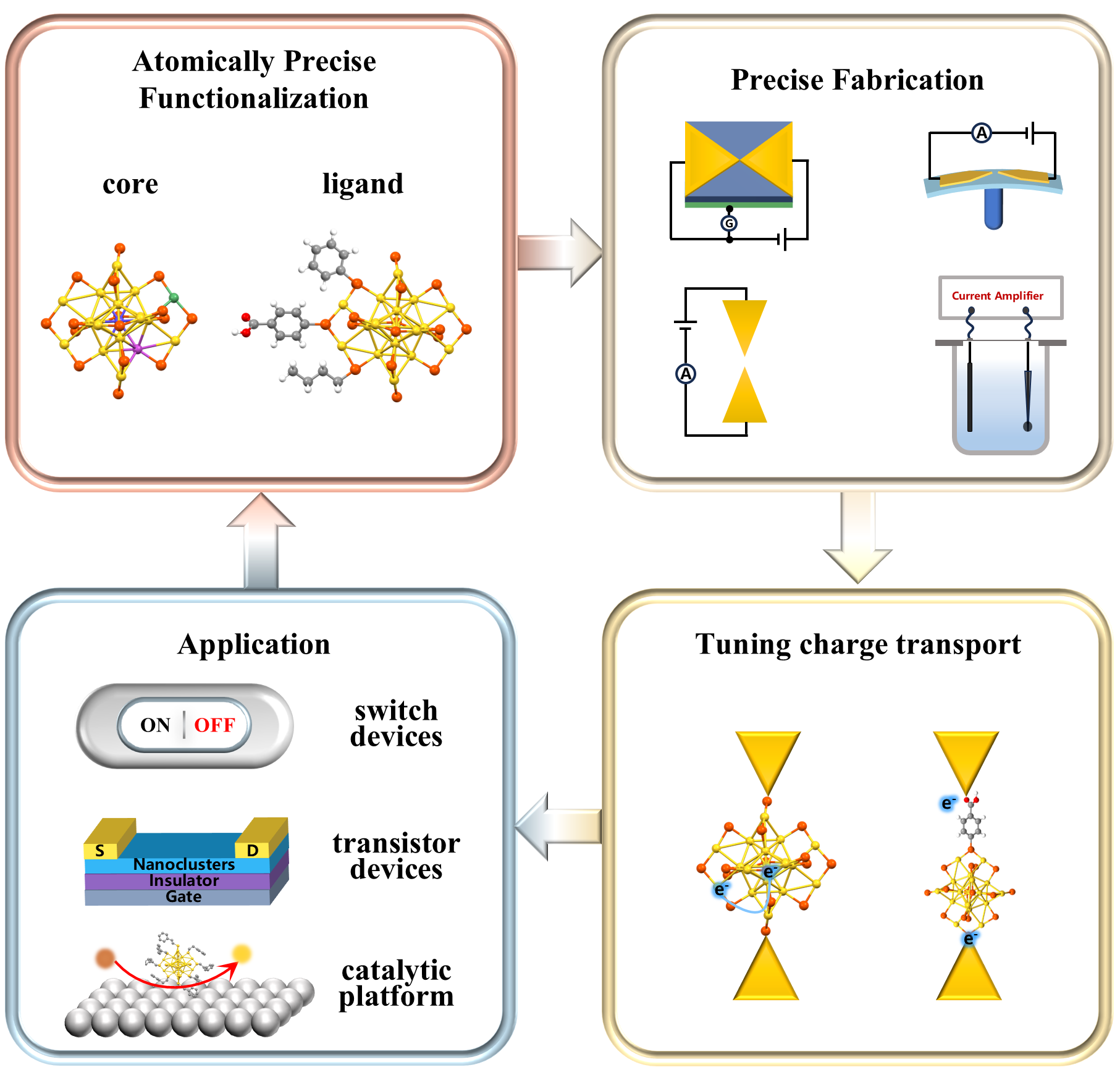
Although significant progress has been made in research on single-cluster devices, the field still lacks a systematic framework to connect the entire chain from "precise synthesis" to "functional applications." This lack of systematization has, to some extent, constrained further development and disciplinary integration in this interdisciplinary field. To address this, this review aims to systematically summarize and analyze recent academic advances in the precise fabrication of single-metal nanocluster devices and their optoelectronic applications, while outlining future development directions and prospects. The specific content includes the following five aspects: (1) A brief summary of precise synthesis methods for functionalized metal nanoclusters to establish a material foundation for device construction; (2) A systematic review of current major fabrication methods for single-cluster devices; (3) An in-depth analysis of research progress on electron transport characteristics at the single-cluster scale; (4) A comprehensive analysis of application examples of single-cluster devices in the field of optoelectronic science; (5) A full summary of challenges facing single-cluster device research and an outlook on their future development directions.

2 Precise Synthesis of Functionalized Metal Nanoclusters

Achieving atomically precise synthesis of metal nanoclusters is a prerequisite for revealing their structure-activity relationships and expanding their applications in catalysis, biomedicine, and optoelectronic devices.[28-30]. Traditional synthesis methods such as the one-pot method[31], the Brust-Schiffrin two-phase method[32-33], the solid-state method[34], and the gas-phase method[35]have laid the foundation for cluster research; their synthetic routes have been summarized in detail in other reviews[36-40], and will not be elaborated upon here. We focus herein on how to optimize the optoelectronic properties of clusters through their precise synthesis. Based on the typical "metal core-organic ligand shell" structural feature of clusters, the key to functionalization lies in the precise regulation or modification of their metal cores or ligand shells. Among these, metal core doping is one of the most effective methods for regulating the electronic structure, geometric configuration, and stability of clusters. Meanwhile, ligand functionalization can finely tune the surface/interface properties and energy level structures of clusters[41-42]. This section will briefly summarize research progress in achieving precise synthesis of metal nanoclusters via two approaches: metal core doping and ligand functionalization. It will focus on exploring how these strategies enable targeted optimization of cluster optoelectronic properties, thereby providing well-defined, optoelectronically controllable functional building blocks for the subsequent precise fabrication of single-cluster devices.

2.1 Metal core doping

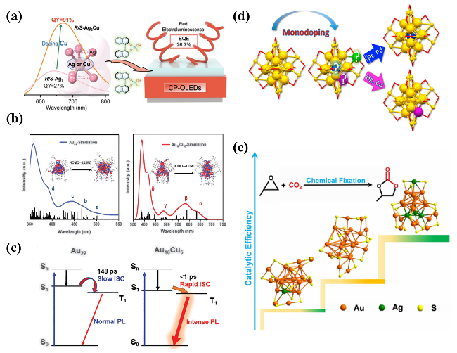
Metal core doping refers to the precise introduction of heterogeneous metal atoms into a metal core framework, achieving direct regulation of the cluster's electronic structure, geometric configuration, and stability. Precisely controlling the number of doped atoms is the primary prerequisite for the precise synthesis of metal nanoclusters; it directly determines the cluster's electronic structure and geometric configuration, thereby influencing its intrinsic optoelectronic properties.[43-46]. In the process of metal core doping, the type of doped atom significantly affects the quantity of doping. Taking the icosahedral Au25(SR)18cluster (Au = gold, SR = thiolate ligand) as an example, when doping with Pd (palladium), Pt (platinum), Cd (cadmium), or Hg (mercury), the cluster tends to incorporate only a single heteroatom.[47]. The team of Zhikun Wu[48]introduced single Pd and Pt atoms into Au25(PET)18(PET = SCH2CH2Ph), successfully synthesizing Au24Pd(PET)18and Au24Pt(PET)18clusters. Spectral analysis indicated that single-atom doping significantly altered the cluster's electronic structure, subsequently changing the magnetism of the cluster from paramagnetic before doping to diamagnetic after doping. The team of Zhongning Chen[49]prepared Ag6Cu clusters by doping Cu(I) (Cu = copper) into Ag7(Ag = silver) clusters; their photoluminescence quantum yields (PLQY) increased from 27% for Ag7to 91% for Ag6Cu (Figure 1a). This is primarily due to the enhanced structural rigidity of the cluster after Cu doping, as well as accelerated rates of intersystem crossing (ISC) and reverse intersystem crossing (RISC). Circularly polarized organic light-emitting diodes (LEDs) fabricated based on this material achieved an external quantum efficiency (EQE) of up to 26.7%, superior to most red organic LEDs. Doping with a single heteroatom has certain limitations in regulating the electronic and geometric structures of clusters; increasing the number of doped atoms can achieve more significant regulation of the cluster's geometric structure. The team of Quanming Wang[50]doped six Cu atoms into Au22, increasing the cluster's PLQY from 9% to nearly 100%; this is because after doping with six Cu atoms, the cluster structure contracted, the highest occupied molecular orbital-lowest unoccupied molecular orbital (HOMO-LUMO) energy gap decreased, and the ISC rate accelerated (Figures 1b, c). This work provides important material and methodological support for the development of ultra-high brightness and high-efficiency single-cluster electroluminescent devices.
图1 金属核掺杂:(a) 在Ag7团簇中精准掺入1个Cu原子制备高发光LEDs[49];(b~c) 在Au22团簇中精确掺入6个Cu原子,减小团簇的HOMO-LUMO间隙[50];(d) 在Au25团簇中固定位点掺入Pt、Pd、Cd、Hg原子[51];(e) Au团簇中不同位点掺入Ag原子实现高效催化[52]

Fig.1 Metal core doping. (a) Precise doping of one Cu atom in Ag7 cluster to prepare high-luminescence LEDs[49]. Copyright 2024, Wiley‐VCH GmbH. (b~c) Precisely incorporating six Cu atoms into Au22 cluster to reduce the HOMO-LUMO gap of the cluster[50]. Copyright 2024, The American Association for the Advancement of Science. (d) Locality-specific incorporation of Pt, Pd, Cd, and Hg atoms into Au25 clusters[51]. Copyright 2019, American Chemical Society. (e) Incorporating Ag atoms at different sites in Au clusters to achieve efficient catalysis[52]. Copyright 2021, Wiley‐VCH GmbH

Precise control of doping sites is another key dimension for revealing the structure-activity relationships of clusters and achieving targeted performance regulation. The Maran team[51]combined nuclear magnetic resonance spectroscopy and electrochemical analysis to precisely resolve the site selectivity of different dopant atoms in Au25: Pt and Pd prefer to occupy the central position of the icosahedral Au13core, while Cd and Hg tend to dope at the icosahedral shell sites (Figure 1d). This difference in site selectivity is mainly attributed to the inherent physicochemical properties of the dopant atoms, including atomic radius and electronegativity. Professor Zhu Yan's team[52]compared the catalytic performance of a series of Ag-doped Au clusters with different doping sites in the cycloaddition reaction of CO2with epoxides. Experimental results show that the Au19Ag4cluster with fully exposed silver sites exhibits the best catalytic activity and stability, while the Au20Ag1cluster with partially exposed silver sites has the lowest catalytic efficiency. This is mainly because the Au19Ag4cluster possesses Ag sites with high structural openness and partial positive charge, which can effectively promote the adsorption of CO2and the ring-opening of epoxides (Figure 1e). Such precise design and regulation of active sites are of great significance for constructing high-performance single-cluster catalytic sensors and energy conversion devices.
In summary, metal core doping enables atomically precise manipulation of the electronic structure and geometric configuration of clusters by precisely controlling the number, type, and sites of dopant atoms, laying a solid material foundation for the directional optimization of cluster optoelectronic properties and the design of high-performance single-cluster optoelectronic devices.

2.2 Ligand functionalization

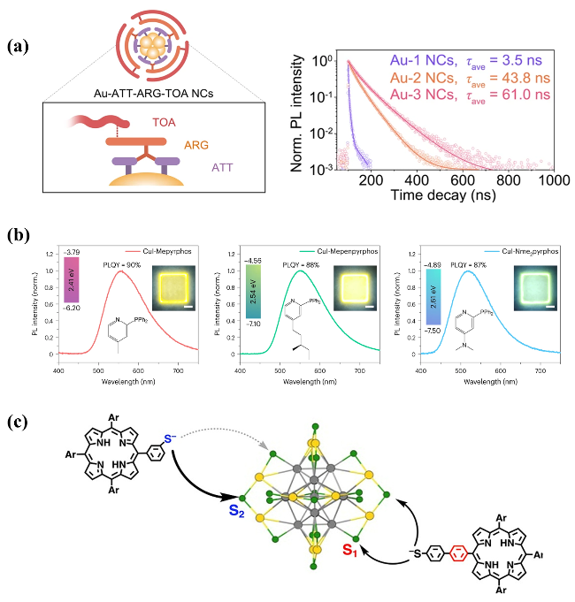
As the interface where ligands directly interact with the external environment for clusters, their precise modification is one of the core strategies for regulating cluster interfacial properties and optoelectronic performance[53-55]. Precise ligand modification mainly focuses on atomic-level control over the number of ligands and substitution sites, typically achieved by regulating reaction kinetics and thermodynamics. Professor Xie Jianping's team[56]developed a redox reaction-guided surface engineering method, achieving reversible addition/removal of single ligands on Au25clusters, clarifying the reversible interconversion mechanism between [Au25(MHA)18]-(MHA = 6-mercaptohexanoic acid) and [Au25(MHA)19]0. Studies indicate that after adding an extra thiol ligand, the stability of the ligand shell of Au25clusters changes; this change is speculated to stem from alterations in the ligand shell packing mode and internal stress. In addition to precisely doping the original ligands in the cluster by number, the team also utilized 6-aza-2-thiothymine, L-arginine, and tetraoctylammonium as ligands to perform stepwise modification of Au10clusters via self-assembly (Figure 2a), significantly improving the photoluminescence efficiency of the clusters[57]. This research demonstrates that precise numerical control and functional modification of surface ligands on clusters can achieve specific optimization of cluster photophysical properties. In application research oriented towards devices, Professor Yao Hongbin's team[58]precisely introduced ligands with different electron-donating abilities into copper iodide clusters, finding that as the electron-donating ability of the ligands increased (dimethylamino > pentyl > methyl), the emission wavelength redshifted and the bandgap decreased, proving that ligand electronic effects can precisely regulate emission color (Figure 2b). The PLQY of the modified material approached 90%, and the EQE of LEDs fabricated based on this material was significantly superior to most lead-free metal halide LEDs, fully demonstrating the great potential of ligand functionalization in realizing efficient and spectrally tunable single-cluster light-emitting devices.
图2 配体功能化:(a) 自组装逐层修饰Au10团簇提升其光致发光效率[57];(b) 在碘化铜簇中精准修饰不同给电子能力的配体以调控发光颜色[58];(c) 利用配体空间位阻的差异实现配体掺杂位点的特异性调控[62]

Fig.2 Ligand functionalization. (a) Self-assembly layer-by-layer modification of Au10 clusters to enhance their photoluminescence efficiency[57]. Copyright 2023, Springer Nature. (b) Precise modification of ligands with different electron-donating abilities in copper iodide clusters to regulate the luminescence color[58]. Copyright 2024, Springer Nature. (c) Spatial steric hindrance of ligands induced site-specific ligand exchange[62]. Copyright 2022, American Chemical Society

Different ligand sites on the cluster surface possess specific chemical microenvironments, electronic coupling strengths, and spatial accessibility[59-60]. Achieving precise modification of ligands at specific sites is of great significance for revealing the mechanism of cluster-environment (e.g., electrode) interface interactions and optimizing the performance of single-cluster devices. The Ackerson team[61]controlled the reaction time to utilizep-BBT (p-BBT = p-bromobenzenethiol) for Au102(p-MBA)44 clusters (p-MBA = p-mercaptobenzoic acid) to perform ligand exchange. By employing a kinetic control strategy, the ligand exchange reaction was made to occur preferentially at specific sites with kinetic advantages, achieving precise control over the ligand modification sites. The specificity of doping sites can also be achieved through the physicochemical properties of the doping ligands themselves. The Teranishi team[62]exchanged ligands between [Au25(SC2Ph)18]-(SC2Ph = 2-phenylethanethiol) and porphyrin thiolates (Por) with different steric hindrances, finding that bulky porphyrin thiolates are more likely to exchange to positions on the cluster surface with smaller steric hindrance, namelyFigure 2c, at the top S2 site of the cluster's staple structure shown. This is the result of the combined effects of steric repulsion and thermodynamic stability: the larger spatial openness of the S2 site reduces steric conflicts between ligands, enabling bulky ligands to undergo ligand exchange reactions in a lower-energy configuration and remain stably on the cluster surface. Niihori et al.[63]reacted Au24Pd(SC2Ph)18 clusters with different ligands. The results indicated that during ligand exchange, the reaction occurs preferentially at thiolate ligand sites directly connected to the metal core. This is mainly due to the strong electronic structure coupling between the ligands at these sites and the metal core, small steric hindrance, and low reaction energy barriers. Therefore, introducing functional ligands at highly reactive sites can directly and efficiently regulate the electron density of the metal active centers and optimize the carrier mobility at the cluster-electrode interface.
In summary, the precision of ligand functionalization is primarily reflected in the accurate control over the number and sites of modification. By regulating the number and sites of ligand modification, it is possible to enhance the intrinsic optoelectronic properties of clusters, which is of decisive significance for improving the charge transport efficiency, interface stability, and optoelectronic catalytic performance of single-cluster devices.
It should be noted that although the metal core doping and ligand functionalization strategies discussed in this section have mostly been validated in cluster aggregate systems, the regulation of intrinsic properties such as the electronic structure, energy level alignment, and interface stability of individual clusters constitutes the physical basis determining the performance of single-cluster devices. Therefore, the aforementioned precise synthesis strategies provide a critical material foundation for the subsequent performance optimization of single-cluster devices.

3 Fabrication of single-cluster devices

As a functional unit with great potential for building novel optoelectronic devices, how to precisely and controllably connect individual clusters between test electrodes to construct "electrode-cluster-electrode" junctions with well-defined electron transport properties is key to studying the physicochemical properties and applications of single-cluster devices.[64-65]. Next, we summarize the preparation techniques, principles, and characteristics of the most widely used single-metal nanocluster devices based on the junction formation methods of different single-cluster junctions.

3.1 Static Single-Cluster Device – Electromigration Technology

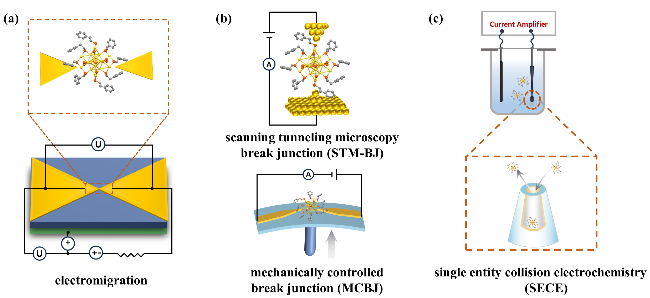
One of the core challenges in precisely fabricating single-cluster devices is constructing electrode gaps to accurately match cluster dimensions. Since most cluster sizes fall within the <2 nm range, the precision of traditional lithography techniques is insufficient to meet these requirements.[66]. Electromigration technology is currently one of the most commonly used techniques for fabricating static single-cluster devices.[67], its core principle utilizes Joule heating and electromigration forces to jointly induce directional migration of atoms within metal nanowires, ultimately resulting in a controlled fracture at a preset location to form electrode gaps on the sub-nanometer to few-nanometer scale (Figure 3a)[68].
图3 单团簇器件的制备技术:(a) 电迁移技术[68];(b) 断裂结技术[69];(c) 单颗粒碰撞技术[70]

Fig.3 Fabrication techniques for single-cluster devices. (a) electromigration technology[68]; (b) break junction technology[69]; (c) single-particle collision technology[70]

Subsequently, the solution containing the target clusters is drop-cast or spin-coated onto prepared nanogap electrodes (mostly gold electrodes). By leveraging terminal functional groups on the cluster surface ligands, such as thiol (—SH) and phosphino (—PR3), covalent bonds are formed with the gold electrodes, allowing individual clusters to spontaneously and selectively bridge the two ends of the nanogap, forming a stable "electrode-cluster-electrode" junction[71]. To improve the precision and success rate of single-cluster bridging, a self-assembled monolayer of molecules or atoms can be pre-modified or deposited in situ on the electrode surface. Single-cluster junctions precisely constructed based on this technology can be further integrated with gate electrodes to form a single-cluster field-effect transistor (FET) structure[72-73], thereby achieving in situ and precise regulation of the cluster's charge state and transport behavior, greatly expanding its applications in fields such as logic operations and sensing.
Single-cluster devices fabricated via electromigration technology are static devices. Their significant advantages include highly stable electrode structures, facilitating precise measurements under extreme conditions such as low temperatures. Furthermore, the fabricated single-cluster devices exhibit good reproducibility and are easy to integrate. Therefore, this remains one of the most commonly used precise fabrication techniques for current research on static single-cluster devices. However, this method also has drawbacks, including reliance on complex micro-nano fabrication processes (resulting in higher costs), a relatively low success rate for single-cluster bridging, and difficulty in precisely controlling the electrode gap size.

3.2 Dynamic single-cluster device

3.2.1 Fracture Knot Technology

Break junction technology is currently the most commonly used technique for studying the electronic properties of single clusters, mainly including two types: scanning tunneling microscopy break junction (STM-BJ) and mechanically controlled break junction (MCBJ).[69].
The working principles of the two break junction techniques are identical; their core involves controlling the electrode spacing to form a stable connection between a single cluster and the two electrodes, followed by slowly increasing the electrode spacing until the connection breaks. This cycle is repeated at high speed to accumulate a large amount of data (Figure 3b). The core difference between them lies in the precise control mechanism for the electrode gap. For STM-BJ, an atomic-level contact is formed by bringing the STM tip close to the metal substrate, and then the tip is slowly retracted to break the contact and form a nanogap (upper part of Figure 3b); the tip motion is controlled by piezoelectric ceramics, achieving sub-angstrom resolution[74]. For MCBJ, the electrode pair is fixed on a flexible substrate, and a mechanical pusher underneath controls the deformation of the substrate to precisely regulate the opening and closing of the electrode gap (lower part of Figure 3b), enabling highly stable and low-noise measurements[75].
In the break-junction process, the key to constructing single-cluster junctions is achieving a stable connection between the single cluster and the electrodes. Currently, gold electrodes are the most commonly used, and there are mainly three methods for stably connecting single-cluster junctions to gold electrodes. The first is ligand anchoring: utilizing functional groups at the ends of ligands on the cluster surface, such as —SH, amino (—NH2), halogens, etc., to form strong covalent/coordination bonds with the metal electrode[76]. The second is interface engineering: pre-modifying the electrode substrate with a monolayer to capture and fix individual clusters through electrostatic interactions or supramolecular interactions[77]. The third is metal bonding: for clusters with weak ligands or exposed metal sites, their metal cores can directly form metal-metal bonds with the electrode[78].
STM-BJ and MCBJ complement each other in the study of single-cluster electronics; STM-BJ enables dynamic control with ultra-high spatial resolution[79-80], elucidating the dynamic evolution mechanisms of single clusters; whereas MCBJ offers strong anti-interference capabilities and long gap lifetimes, enabling stable long-term testing[80-81]. Furthermore, both techniques exhibit excellent adaptability to different temperature environments. The synergistic development of these two technologies has significantly advanced the full-chain research process in single-cluster electronics, from exploring fundamental charge transport mechanisms to validating functional devices.

3.2.2 Single entity collision electrochemistry (SECE)

SECE is an emerging dynamic analysis technique with ultra-high spatiotemporal resolution[82-83]. The principle of this technique involves utilizing individual nanoclusters to randomly collide with the surface of a nano-electrode via Brownian motion, monitoring the transient current signals generated during this process to achieve real-time, in-situ analysis of the electrochemical activity of single nanoclusters.
The key to the SECE experiment lies in preparing highly sensitive nanoelectrodes. Specifically, electrodes with nanoscale tips are first fabricated in quartz capillaries using a laser puller. Subsequently, a conductive carbon film is deposited on the inner surface of the nanoelectrode via chemical vapor deposition, forming a carbon nanoelectrode (CNE) with high conductivity and stability.[70]. The nanoscale dimensions of the CNE determine the lower size limit for detectable clusters. During the experiment, the prepared CNE is immersed in an electrolyte containing the target clusters. The clusters diffuse randomly via Brownian motion and collide with or adsorb onto the CNE surface, achieving single-cluster capture (Figure 3c). To overcome the issues of weak signals and short durations associated with individual collision events, researchers have developed electrode interface functionalization strategies. By electrochemically depositing polymer films on the CNE surface, nitrogen-doped (N-CNE), sulfur-doped (S-CNE), and nitrogen-sulfur co-doped (NS-CNE) carbon nanoelectrodes are formed.[84], this method not only extends the dwell time of collisions but also enhances the interaction between clusters and the electrode, thereby significantly improving signal intensity and stability.
In summary, although SECE technology has drawbacks such as complex electrode preparation processes and difficulties in large-scale application, its advantages of high sensitivity and high spatiotemporal resolution, which enable real-time, in-situ monitoring of the electrochemical reaction activity of single clusters directly in room-temperature solution environments, are of significant importance for studying the catalytic reaction mechanisms and charge transfer characteristics of single clusters.
In summary, electromigration technology is suitable for constructing static, highly stable single-cluster devices. This technology is inherently compatible with planar back-gate electrode structures, enabling efficient gate voltage modulation and providing an ideal platform for studying the electrical properties of clusters. STM-BJ and MCBJ, based on a large number of repetitive tests within a short time frame, can rapidly obtain statistical results of the electrical properties of individual clusters; thus, they are more suitable for studying dynamic, high-resolution charge transport behaviors, particularly for in-situ analysis of interface coupling and structural evolution. Meanwhile, SECE technology offers unique spatiotemporal resolution advantages in solution environments, making it suitable for real-time monitoring of catalytic processes and electrochemical behaviors. Researchers can reasonably select the corresponding fabrication scheme for single-cluster devices based on specific application goals and testing environments.

4 Electrical transport behavior of single-cluster devices

The precise construction of single-cluster devices lays a solid foundation for in-depth investigation of their intrinsic electrical transport properties. In a single-cluster junction, the electrical transport behavior is jointly determined by two key structural hierarchies of the "electrode-cluster-electrode" junction: the interfacial coupling between the cluster and the electrodes (the cluster-electrode interface layer) and the internal structure of the cluster itself (the cluster layer). Precisely resolving and regulating the influence mechanisms of these two hierarchies is crucial for revealing the relationship between cluster structure and device performance. This section will systematically elucidate the influence mechanisms of these two key structural hierarchies, namely the "cluster-electrode interface layer" and the "cluster layer," on the electrical transport properties of single-cluster junctions, and will focus on discussing strategies and mechanisms for achieving directional optimization of electrical transport behavior through precise regulation of the aforementioned structural hierarchies.

4.1 Regulation of electron transport behavior in single-cluster junctions by the cluster-electrode interface

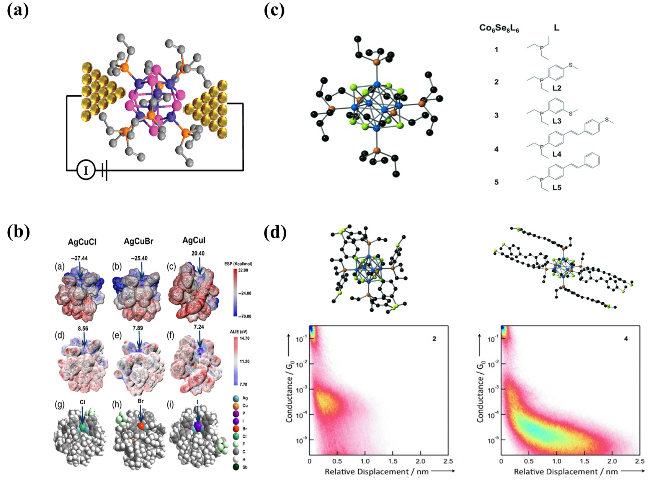
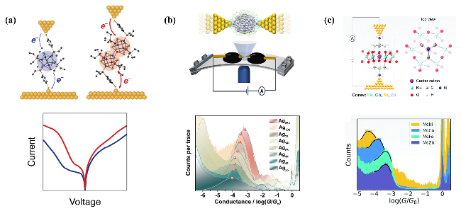
The precise construction and regulation of the cluster-electrode interface are core factors determining the electron transport properties of single-cluster junctions. Among these, the type of anchoring element at the cluster-electrode interface plays a decisive role in the electrical transport process. Taking chalcogen elements, which are most widely used in clusters, as an example: as elements that can coordinate with both metal elements within the cluster and the working electrode, the type of chalcogen element significantly affects the electrical transport behavior of single-cluster junctions. Professor Nuckolls' research group[78]synthesized a series of isostructural cobalt chalcogenide clusters: (1) Co6Te8(P(C2H5)3)6 (Co = cobalt, Te = tellurium); (2) Co6Se8(P(C2H5)3)6 (Se = selenium); (3) Co6S8(P(C2H5)3)6. STM-BJ results show that conductance follows the order Te > Se > S (Figure 4a). Cyclic voltammetry (CV) characterization demonstrates that Te-anchored clusters possess the lowest oxidation potential and the highest HOMO energy level. Combined with Density Functional Theory (DFT) calculations, it was found that the HOMO is concentrated on Te atoms. According to the Hard and Soft Acids and Bases (HSAB) theory, among the three elements, the softest base Te achieves optimal orbital overlap with Au, effectively reducing the interfacial barrier and thereby resulting in higher cluster conductance; conversely, the hardest base S leads to the lowest cluster conductance value. In addition to chalcogen elements, halogens as anchoring elements can also directly regulate the electrical transport behavior of single-cluster junctions. The team of Hong Wenjing[85]synthesized AgCuX clusters coordinated by different halogens (X = Cl (chlorine), Br (bromine), I (iodine)) and compared the influence of different halogens on the electrical transport behavior of single-cluster junctions. Halides possess lone pair electrons; the electrostatic potentials (ESP) around them exhibit negative potential, and their Average Local Ionization Energy (ALIE) values are low. This allows them to form stable connections with unsaturated sites on Au electrodes through electrostatic attraction and chemical bonding (Figure 4b). Raman spectroscopy confirmed the existence of Au—X bonds. ESP-ALIE analysis further indicated that halogen atoms and their surrounding regions are the most active anchoring areas. Thus, the authors determined that halogens can serve as anchoring sites to form stable connections with gold electrodes. Moreover, the coupling strength sequence with gold electrodes is Au—Cl < Au—Br < Au—I. The conductance sequence of the three clusters is consistent with the coupling strength, namely AgCuCl (3.88 nS) < AgCuBr (8.30 nS) < AgCuI (14.43 nS). This is because from Cl to I, the atomic radius increases and electronegativity decreases, improving orbital overlap with Au, enhancing interfacial coupling, and increasing electron transmission probability. Furthermore, in this work, through rational structural design utilizing the exposed lone pair electrons of halogens, the authors achieved direct bonding between the electrode and the cluster interface. This avoided the system complexity caused by multi-site anchoring within the cluster, resulting in a more concentrated conductance distribution and significantly improving the clarity and reliability of the device structure. At the cluster-electrode interface, besides the type of element at the anchoring site, the steric effect of ligands is also an important factor regulating the electrical transport behavior of the cluster-electrode interface. Xavier et al.[86]used Co6Se8(PEt3)6clusters as a model, introducing ligands containing sulfur-methyl groups (L2~L4) into them. The phosphorus end of the ligand coordinates with cobalt, while the sulfur-methyl end coordinates with the gold electrode. Ligands L2 and L4 adopt a para-substituted configuration (Figure 4c). DFT calculations revealed that para-substituted ligands (L2, L4) can form effective π-conjugated electron pathways connecting the cluster core with the anchoring group, thereby causing clusters 2 and 4 to exhibit distinct conductance peaks (Figure 4d). In contrast, ligand L3 is meta-substituted; in diethyl-3-(thiomethyl)phenylphosphine, the 3-(thiomethyl)phenyl group cannot rotate around the P—C bond to form an effective conductive pathway, resulting in no significant conductance signal for cluster 3. Comparing clusters 1~3 reveals that the ligand substitution position can affect electrical transport efficiency by controlling the spatial orientation of the electron transmission path. The Nuckolls research group[78]also compared Co6Te8(P(n-Bu)3)6(P(n-Bu)3 = tri-n-butylphosphine) and Co6Te8(P(C2H5)3)6 , two types of Co6Te8clusters with ligands of different steric hindrance, finding that as the steric hindrance of the ligands increases, the cluster conductance decreases significantly. This is attributed to the fact that bulky ligands hinder the orbital overlap between the lone pair electrons of Te and the gold electrode, thereby weakening the interfacial coupling strength.
图4 团簇-电极界面对单团簇结电输运能力的调控:(a) Co6Te8、Co6Se8、Co6S8的单团簇结模型示意图[78];(b) AgCuCl、AgCuBr、AgCuI的静电势(上)平均局部电离能(中)和团簇模型图(下)[85];(c) Co6Se8L6团簇的结构模型及对应的5种配体的结构[86];(d) Co6Se8L6中,L2和L4对应团簇的结构及对应的二维电导-距离直方图[78]

Fig.4 Modulation of the electrical transport properties of single cluster junctions at the cluster-electrode interface. (a) Schematic diagrams of single-cluster junction models for Co6Te8, Co6Se8, and Co6S8[78]. Copyright 2011, American Chemical Society. (b) Electrostatic potential (top), average local ionization energy (middle), and cluster model diagrams (bottom) for AgCuCl, AgCuBr, and AgCuI[85]. Copyright 2022, Chinese Chemical Society. (c) Structural model of the Co₆Se₈L₆ cluster and the structures of the five corresponding ligands[86]. Copyright 2012, Wiley‐VCH GmbH. (d) Structures of the clusters corresponding to L2 and L4 in Co6Se8L6 and their corresponding two-dimensional conductance-distance histograms[78]. Copyright 2011, American Chemical Society

In addition, the solvent environment and ligand length[87-90]and other factors can also regulate the cluster-electrode interface coupling and electrical transport behavior to varying degrees. In summary, by precisely designing the types of anchoring elements at the cluster-electrode interface (to regulate coupling strength) and the spatial configuration/steric hindrance of ligands (to regulate the geometric structure and electron transport pathways at the interface), researchers can achieve directional and predictable regulation of the electrical transport behavior of single-cluster junctions. Specifically, "directional" refers to the systematic adjustment of parameters such as conductance and coupling strength of single-cluster junctions through rational design of the anchoring element types and ligand spatial configurations at the cluster-electrode interface; "predictable" refers to predicting the electrical transport behavior of clusters with different structures based on existing experimental results combined with theoretical simulations, providing a solid theoretical foundation for designing high-performance single-cluster optoelectronic devices.

4.2 Regulation of electrical transport behavior in single-cluster junctions by the intrinsic structure of clusters

The intrinsic structure of clusters (such as size and atomic composition) is the intrinsic determining factor of their electrical transport behavior. In the synthesis and design of clusters, although macroscopic studies have shown that structural changes significantly affect properties such as catalysis and luminescence of clusters[91-94], the average effects at the macroscopic scale and size heterogeneity seriously hinder the precise construction of their structure-activity relationships[95]. However, the construction of single-cluster devices provides an ideal platform for revealing the regulation of intrinsic structural features, such as size effects and atomic doping, on the electrical transport behavior of clusters at the atomic level.
The size of the metal core affects its quantum confinement effect and electronic density of states, thereby enabling the regulation of its electrical transport capability. Gunasekaran et al.[96]synthesized model clusters with a single Co core and Co core dimers. Comparison revealed that increasing the size of the cluster metal core can significantly enhance the device current and lead to current saturation phenomena (Figure 5a). The authors pointed out that the increase in metal core size reduces the reorganization energy of the system and leads to a denser distribution of energy levels, synergistically enhancing the electron tunneling probability and transport efficiency, resulting in current enhancement and saturation behavior. Subsequently, the Hong Wenjing group compared Ag clusters with continuously varying sizes[97](Agx, wherex = 25, 43, 44, 63, 78, 136, 141, and 374) regarding their electrical transport behavior. They found that the size effect of the metal core in single-cluster junctions exhibits a trend completely opposite to that in organic single-molecule junctions; specifically, conductance increases monotonically with increasing cluster size (Figure 5b), with a conductance decay constant of approximately 0.4 nm-1. Experiments and theoretical calculations indicate that the HOMO-LUMO gap of Agxclusters decreases significantly with increasing metal core size, and the coupling between the cluster and electrodes is enhanced, leading to increased conductance. On the other hand, within the same cluster, conductance also exhibits an increasing trend with the increase in the linear distance between electrode anchoring sites. This study demonstrates that by precisely controlling the cluster size, the gap magnitude and interface coupling strength can be effectively regulated, thereby achieving directional modulation of its electrical transport behavior.
图5 团簇本征性质对单团簇结电输运能力的调控:(a) 单体金属核簇Co6Se8和二聚体金属核簇Co12Se16的单团簇结模型示意图及对应的I-V曲线(蓝色代表Co6Se8,红色代表Co12Se16[96];(b) 测试Agx电导的单团簇结模型示意图及对应的一维电导统计图[97];(c) Mo团簇的单团簇结模型及掺入不同杂原子对应的一维电导统计图[98]

Fig.5 Modulation of the electrical transport properties of single cluster junctions by intrinsic properties of individual clusters. (a) Schematic diagram of the single-cluster junction model for the monomeric metal-core cluster Co6Se8 and the dimeric metal-core cluster Co12Se16, along with their corresponding I-V curves (blue for Co6Se8, red for Co12Se16[96]. Copyright 2020, American Chemical Society. (b) Schematic diagram of the single-cluster junction model for testing the conductance of Agx and the corresponding one-dimensional conductance statistics[97]. Copyright 2022, American Chemical Society. (c) Single-cluster junction model for Mo clusters and the corresponding one-dimensional conductance statistics for clusters doped with different heteroatoms[98]. Copyright 2021, The Royal Society of Chemistry

Introducing heteroatoms into clusters for atomic-level precise doping is a powerful means to regulate their electronic structures. Yuan et al.[98]utilized STM-BJ technology to investigate the influence of central atom doping on the electrical transport behavior of Anderson-type polyoxometalate (POM) clusters. They synthesized four types of POM clusters with different central metal atoms: MoFe, MoCo, MoNi, and MoZn. Experimental results demonstrated that by changing the central metal atom, the conductance of POM clusters could be directionally regulated within an order of magnitude (Figure 5c). Furthermore, by introducing a temperature gradient in the STM-BJ, the authors measured the thermoelectric potential of the clusters and obtained their Seebeck coefficients. They found that the Fermi levels of the MoFe, MoNi, and MoZn clusters were close to the HOMO, while the Fermi level of the MoCo cluster was close to the LUMO. Combined with theoretical calculations, it was revealed that the substitution of the central atom led to a non-uniform reconstruction of the electrostatic potential distribution within the clusters. This electron structure change induced by atomic-level precise doping not only directly regulated the cluster conductance but also affected its bias dependence and thermoelectric response. This study directly correlated atomic-level doping, fine-tuning of electronic structures, and multi-dimensional transport properties at the single-cluster level, providing atomic-scale insights for designing functional nanoelectronic devices based on doped clusters.
In summary, the intrinsic structure of clusters is a core factor regulating the electrical transport behavior of single-cluster devices. These structure-activity relationships obtained at the single-cluster level not only deepen the understanding of fundamental laws of charge transport at the nanoscale, but also lay a solid theoretical and experimental foundation for precisely customizing single-cluster devices with specific optoelectronic properties at the atomic level, effectively promoting the application of single-cluster devices in fields such as nanoelectronics, quantum information processing, and energy conversion.

5 Application of single-cluster devices

The rich charge transport characteristics exhibited by single-cluster junctions under the regulation of interface coupling and intrinsic cluster structure provide an atomic-precision design foundation for developing novel functional nanodevices.[99]This section will summarize current research progress in functional applications of single-cluster devices, focusing on their applications in switching devices, transistor devices, and in-situ catalytic detection.

5.1 Single-cluster switching device

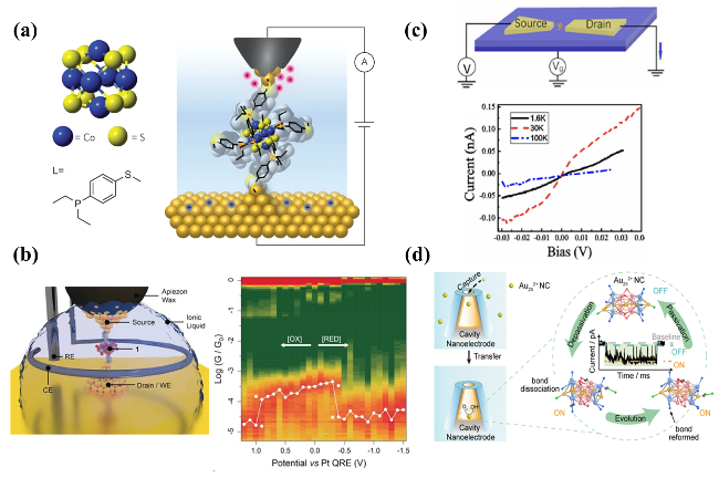
The significant Coulomb blockade effect in clusters lays the theoretical foundation for realizing electrically controlled switching devices. Based on this effect, changing the charge state of clusters through external regulation can achieve the "on" and "off" states of the device[15]. Lovat et al.[100]used STM-BJ technology to perform bias regulation on Co6S8L6 clusters (L = diethyl-4-(methylthio)phenylphosphine). They found that charge transport was significantly suppressed within a bias range of 360 to -450 mV (Figure 6a), while outside this range, the current of the single-cluster junction increased significantly with bias. The maximum switching ratio of single-cluster switching devices designed based on this bias regulation mechanism can reach 600. The core strategy for achieving switching functionality is to regulate the charge state of clusters through external stimuli. In addition to bias regulation, electrochemical potential regulation is also an effective means to achieve switching functionality. The Vezzoli team[101]prepared single-cluster junctions via the STM-BJ method, which exhibited obvious conductance responses under electrochemical potential control. As the potential moved from zero to negative values, the conductance increased slightly; when the potential reached approximately -0.3 V, the cluster accepted an electron, its charge state changed from -3 to -4, and the conductance decreased significantly. When the potential moved in the positive direction, the cluster charge state switched from -3 to -2, and the conductance dropped to the lowest level. This electrochemical potential regulation achieved reversible switching among three charge states: -4, -3, and -2 (Figure 6b), with the switching ratio between adjacent states exceeding one order of magnitude. Whether through bias regulation or electrochemical potential regulation, the essence of both is regulating the charge state of clusters to achieve the injection or removal of single electrons. These works fully demonstrate that utilizing single clusters holds promise for designing high-performance, multi-state molecular switches to achieve single-electron manipulation at the atomic level.
图6 单团簇器件的应用:(a) 利用Co6S8L6电荷态的偏压响应特性设计的单团簇开关器件模型示意图[100];(b) 栅压调控单团簇开关器件模型及对应电化学调控窗口内的电导热图[101];(c) 基于Au13团簇构建的单团簇晶体管器件及不同温度下对应的I-V曲线[72];(d) 基于Au252+构建的SECE器件原位表征ORR反应的模型及对应的结构-电流响应示意图[84]

Fig.6 Applications of single-cluster devices. (a) Schematic diagram of a single-cluster switching device model designed by modulating the charge state of Co6S8L6 using bias voltage[100]. Copyright 2017, Springer Nature. (b) Model of a gate voltage-modulated single-cluster switching device and the corresponding thermal map of conductance within the electrochemical modulation window[101]. Copyright 2020, Wiley‐VCH GmbH. (c) Single-cluster transistor device constructed based on an Au13 cluster and the corresponding I-V curves at different temperatures[72]. Copyright 2024, American Chemical Society. (d) Model for in situ characterization of the ORR reaction using a SECE device constructed based on Au252+ and the corresponding structure-current response diagram[84]. Copyright 2024, American Chemical Society

5.2 Single-cluster transistor device

Applying single-cluster devices to the field of transistors relies on utilizing the quantum effects of clusters to achieve single-electron control. Such devices are typically fabricated using techniques like electromigration or chemical deposition combined with "soft landing." In 2017, the team led by Song Fengqi first conducted electrical transport measurements on Au13clusters[72], observing Coulomb blockade behavior in this cluster at 1.6 K.I-V(Irepresents current,Vrepresents voltage) curves show that the conductivity of Au13is suppressed at low bias voltages, followed by step-like current jumps at higher voltages; the switching ratio of this transistor approaches 5 (Figure 6c). When the temperature rises to 100 K, theI-Vcurve exhibits linear behavior, indicating that Coulomb blockade disappears at temperatures above 100 K. It is worth noting that the electrical behavior of the aforementioned transistors was observed at low temperatures, which limits their application at room temperature to some extent. To overcome this limitation, the Vondel team[102], after fabricating nanogaps using electromigration technology, deposited charged aluminum clusters into the electrode gaps via "soft landing" technology, observing the Coulomb blockade effect at room temperature. Its charging energy is 0.14 eV, far greater than the thermal energy at room temperature (approximately 26 meV). This key progress confirms the feasibility of single-cluster-based transistors operating normally at room temperature, marking an important step toward their industrialization and integration.

5.3 Catalytic detection platform based on single-cluster devices

Designing in-situ catalytic detection devices based on single clusters can avoid the averaging effects in traditional catalytic experiments, thereby enabling a more accurate understanding of elementary catalytic reactions at the single-cluster and single-molecule levels, and providing theoretical and experimental guidance for designing efficient electrocatalysts.[103-104].
Ma Wei Team[84]Constructed a dynamic electrochemical device based on single Au252+clusters using single-particle collision electrochemistry and applied it to the oxygen reduction reaction (ORR). This technique successfully captured the dynamic structural evolution of Au252+during the ORR process (Figure 6d): desorption/re-adsorption of surface ligands and conformational changes of the Au259+core jointly caused the device current signal to exhibit characteristic "on-off" state switching and "on" state fluctuations. Recently, the team used the same method to study the catalytic behavior of different single-atom doped silver nanoclusters (M1Ag24, M = Ag, Au, Pt, Cu) in ORR[105]. This platform successfully distinguished the differences in ORR activity among individual M1Ag24clusters caused by different dopant atoms (M) and their positions (central C site or surface O site): clusters doped with Au and Pt at the center exhibited the highest activity, while those doped with Cu on the surface showed lower activity, attributed to the specific regulation of the cluster electronic structure by the dopant atoms. This technology not only provides a powerful tool for atomic-level precise electrochemical research of single clusters but also demonstrates the potential of these devices as fast, high-throughput screening tools for nanocatalysts, greatly expanding the application scope of single-cluster devices.

5.4 Single-cluster light-emitting diode device

When using a single metal nanocluster to fabricate light-emitting diodes, the spectral broadening problem caused by uneven particle distribution in aggregated materials can be effectively avoided. Furthermore, by directionally optimizing the composition, structure, or excitation conditions of the cluster, the luminous efficiency and device stability of single-cluster light-emitting diode devices can be significantly enhanced.
Dickson team[73]Innovatively adopted pulse excitation technology to utilize silver nanoclusters (Ag2-Ag8) in symmetric nanojunctions to achieve single-cluster LED functionality, breaking through the limitation of non-polarity in nanodevices under traditional DC/AC excitation. The team discovered that high-frequency pulse/AC excitation can significantly improve the spectral and thermal stability of electroluminescence in silver nanoclusters, with a spectral width far narrower than that under DC excitation, effectively extending the LED lifespan. This work established a correlation between pulse parameters and electroluminescence performance at the nanoscale, providing effective experimental basis for optimizing the efficiency of nano-LED devices. Furthermore, the highly efficient response of silver nanoclusters in this device lays a solid material foundation for developing high-stability nanoscale light sources.
The optoelectronic applications of the aforementioned single-cluster devices not only highlight their significant value in bridging atomic-level structures with macroscopic device functionalities, but also lay a solid foundation for their future applications in fields such as nanoelectronics, quantum information processing, and precision catalysis.

6 Conclusion and Outlook

Single-cluster devices have become a key bridge connecting nanoscale fundamental research with macroscopic functional device applications. This review systematically outlines the core progress in this field. However, the field still faces numerous critical challenges. For research on high-performance, multifunctional single-cluster devices, future efforts urgently need to conduct in-depth exploration in the following directions.
1) Cluster Stability and Functional Integration: Based on existing ligand systems, develop novel multifunctional responsive ligands to enhance the structural stability of clusters in complex environments and expand their applications in smart responsive devices.
2) Quantitative regulation of interface coupling: In-depth study of the anchoring mechanisms of non-chalcogen elements (such as halogens and nitrogen-containing heterocycles), establishment of a quantitative model for electrode-cluster coupling strength, and realization of precise design of interfacial electronic structures.
3) Promoting the integration of high-performance devices at room temperature: Designing novel cluster materials with high charging energy barriers to accelerate the practical application of room-temperature single-electron devices. Furthermore, developing high-precision techniques for the site-specific assembly of single clusters is crucial, as it holds promise for overcoming the technical bottlenecks in scalable integration associated with existing methods such as electromigration and break junctions.
4) Establish a theory-experiment closed-loop design model: Develop data-driven models integrating machine learning to predict the complex relationships between cluster structure, interface configuration, and transport properties, thereby guiding the integrated design of "targeted synthesis-device construction".
5) Expanding emerging application scenarios: Beyond the aforementioned directions, single-cluster devices demonstrate unique potential in biomimetic artificial enzymes. Metal clusters with atomically precise structures can mimic the active centers and microenvironments of natural enzymes. Their integration into single-cluster devices is expected to achieve highly selective and efficient simulated enzymatic catalytic reactions. This not only enables high-sensitivity biomolecular sensing but also extends to green catalysis fields such as artificial photosynthesis and pollutant degradation, providing a new paradigm for the design of bio-inspired nanodevices.
In summary, research on single-cluster devices is at a critical turning point, transitioning from the exploration of fundamental physical properties to functional integrated applications. Future breakthroughs will highly depend on the deep integration of multidisciplinary approaches, including precision synthesis chemistry, advanced in-situ characterization techniques, and multi-scale theoretical calculations. Through collaborative innovation in "atomic-precision design-controllable preparation-functional integration," single-cluster devices are expected to provide original solutions for fields such as nanoelectronics and quantum computing.
[1]
Yao Q F, Zhu M, Yang Z C, Song X R, Yuan X, Zhang Z P, Hu W P, Xie J P. Nat. Rev. Mater., 2025, 10(2): 89.

[2]
Nimtz G, Marquardt P, Gleiter H. J. Cryst. Growth, 1988, 86(1/4): 66.

[3]
Chen S W, Ingram R S, Hostetler M J, Pietron J J, Murray R W, Schaaff T G, Khoury J T, Alvarez M M, Whetten R L. Science, 1998, 280(5372): 2098.

[4]
Xu T Y, Si W D, Zhang C K, Han B L, Wang Z, Tung C H, Sun D. J. Am. Chem. Soc., 2025, 147(25): 21468.

[5]
Devadas M S, Kwak K, Park J W, Choi J H, Jun C H, Sinn E, Ramakrishna G, Lee D. J. Phys. Chem. Lett., 2010, 1(9): 1497.

[6]
Antonello S, Arrigoni G, Dainese T, De Nardi M, Parisio G, Perotti L, René A, Venzo A, Maran F. ACS Nano, 2014, 8(3): 2788.

[7]
Zhu H S, Li J, Wang J, Wang E K. ACS Appl. Mater. Interfaces, 2019, 11(40): 36831.

[8]
Chen S, Ma H D, Padelford J W, Qinchen W L, Yu W, Wang S X, Zhu M Z, Wang G L. J. Am. Chem. Soc., 2019, 141(24): 9603.

[9]
Yu Y, Luo Z T, Chevrier D M, Leong D T, Zhang P, Jiang D-E, Xie J P. J. Am. Chem. Soc., 2014, 136(4): 1246.

[10]
Wang X J, Yin B, Jiang L R, Yang C, Liu Y, Zou G, Chen S, Zhu M Z. Science, 2023, 381(6659): 784.

[11]
Han Z, Dong X Y, Luo P, Li S, Wang Z Y, Zang S Q, Mak T C W. Sci. Adv., 2020, 6(6): eaay0107.

[12]
Fetzer F, Maier A, Hodas M, Geladari O, Braun K, Meixner A J, Schreiber F, Schnepf A, Scheele M. Nat. Commun., 2020, 11: 6188.

[13]
Galchenko M, Black A, Heymann L, Klinke C. Adv. Mater., 2019, 31(18): 1900684.

[14]
Yuan P, Zhang R H, Selenius E, Ruan P P, Yao Y R, Zhou Y, Malola S, Häkkinen H, Teo B K, Cao Y, Zheng N F. Nat. Commun., 2020, 11: 2229.

[15]
Simatos D, Nikolka M, Charmet J, Spalek L J, Toprakcioglu Z, Jacobs I E, Dimov I B, Schweicher G, Lee M J, Fernández-Posada C M, Howe D J, Hakala T A, Roode L W Y, Pecunia V, Sharp T P, Zhang W M, Alsufyani M, McCulloch I, Knowles T P J, Sirringhaus H. SmartMat, 2024, 5(6): e1291.

[16]
Mao J Y, Jin T Y, Hou X Y, Teo S L, Lin M, Chen J S, Chen W. SmartMat, 2024, 5(6): e1283.

[17]
Song X R, Wei J, Cai X Y, Liu Y Z, Wu F B, Tong S F, Li S H, Yao Q F, Xie J P, Yang H H. ACS Nano, 2024, 18(49): 33555.

[18]
Li S H, Wei J, Yao Q F, Song X R, Xie J P, Yang H H. Chem. Soc. Rev., 2023, 52(5): 1672.

[19]
Chen Y S, Kamat P V. J. Am. Chem. Soc., 2014, 136(16): 6075.

[20]
Xiao G B, Mu X J, Zhou S Y, Zhu L, Peng Y, Liang Q, Zou X X, Zhang J, Zhang L, Cao J. Angew. Chem. Int. Ed., 2023, 62(17):e202218478.

[21]
Kang Q, Zheng Z, Zu Y F, Liao Q, Bi P Q, Zhang S Q, Yang Y, Xu B W, Hou J H. Joule, 2021, 5(3): 646.

[22]
Zhao X Y, Yan Y, Tan M, Zhang S R, Xu X N, Zhao Z B, Wang M N, Zhang X B, Adijiang A, Li Z L, Scheer E, Xiang D. SmartMat, 2024, 5(4): e1280.

[23]
Wei C Y, Xu W, Ji S R, Huang R Y, Liu J Y, Su W Q, Bai J, Huang J L, Hong W J. Nano Res., 2024, 17(1): 65.

[24]
Kano S, Tada T, Majima Y. Chem. Soc. Rev., 2015, 44(4): 970.

[25]
Liu X Y, Gao X W, Xiong L, Li S X, Zhang Y, Li Q, Jiang H, Xu D S. SmartMat, 2024, 5(4): e1224.

[26]
Siu T C, Wong J Y, Hight M O, Su T A. Phys. Chem. Chem. Phys., 2021, 23(16): 9643.

[27]
Yu A, Li S W, Czap G, Ho W. Nano Lett., 2016, 16(9): 5433.

[28]
Chen Y P, Zhou X, Liu X Y, Tang Z H, Wang L K, Tang Q. J. Am. Chem. Soc., 2025, 147(3): 2699.

[29]
Zhou K, Cai W, Tan Y, Zhao Z P, Liu J B. Angew. Chem. Int. Ed., 2022, 61: e202212214.

[30]
Saito Y, Shichibu Y, Konishi K. Nanoscale, 2021, 13(22): 9971.

[31]
Negishi Y, Tsukuda T. J. Am. Chem. Soc., 2003, 125(14): 4046.

[32]
Brust M, Walker M, Bethell D, Schiffrin D J, Whyman R. J. Chem. Soc., Chem. Commun., 1994, 7: 801.

[33]
Li Y, Zaluzhna O, Xu B L, Gao Y, Modest J M, Tong Y J. J. Am. Chem. Soc., 2011, 133(7): 2092.

[34]
Rao T U B, Nataraju B, Pradeep T. J. Am. Chem. Soc., 2010, 132(46): 16304.

[35]
Geng L J, Luo Z X. J. Phys. Chem. Lett., 2024, 15(7): 1856.

[36]
Xu Q H, Gong X K, Zhao Z X, Wang L, Sun J, He J L, Li S M, Shen H. Polyoxometalates, 2025, 4(2): 9140075.

[37]
Zou X J, Kang X, Zhu M Z. Chem. Soc. Rev., 2023, 52(17): 5892.

[38]
Lin Y F, Yang C R, Huang Y F, Chin. Chemical Soc., 2022, 69(8): 1200.

[39]
Shang L, Xu J, Nienhaus G U. Nano Today, 2019, 28: 100767.

[40]
Dhayal R S, van Zyl W E, Liu C W. Acc. Chem. Res., 2016, 49(1): 86.

[41]
Wei X, Lv Y, Shen H L, Li H, Kang X, Yu H Z, Zhu M Z. Aggregate, 2023, 4: e246.

[42]
Wang Y N, Bürgi T. Nanoscale Adv., 2021, 3(10): 2710.

[43]
Li L, Zhang Z C. SmartMat, 2024, 5(4): e1239.

[44]
Fei W W, Tang S Y, Li M B. Nanoscale, 2024, 16(42): 19589.

[45]
Chang W T, Lee P Y, Liao J H, Chakrahari K K, Kahlal S, Liu Y C, Chiang M H, Saillard J Y, Liu C W. Angew. Chem. Int. Ed., 2017, 56(34): 10178.

[46]
Joshi C P, Bootharaju M S, Alhilaly M J, Bakr O M. J. Am. Chem. Soc., 2015, 137(36): 11578.

[47]
Kang X, Li Y W, Zhu M Z, Jin R C. Chem. Soc. Rev., 2020, 49(17): 6443.

[48]
Tian S B, Liao L W, Yuan J Y, Yao C H, Chen J S, Yang J L, Wu Z K. Chem. Commun., 2016, 52(64): 9873.

[49]
Ding X, Shi L, Wang J, Xu L, Zhang L, Chen Z N. Angew. Chem. Int. Ed., 2025, 64: e202417934.

[50]
Shi W Q, Zeng L L, He R L, Han X S, Guan Z J, Zhou M, Wang Q M. Science, 2024, 383(6680): 326.

[51]
Fei W W, Antonello S, Dainese T, Dolmella A, Lahtinen M, Rissanen K, Venzo A, Maran F. J. Am. Chem. Soc., 2019, 141(40): 16033.

[52]
Li G J, Sui X, Cai X, Hu W G, Liu X, Chen M Y, Zhu Y. Angew. Chem. Int. Ed., 2021, 60(19): 10573.

[53]
Zhang B H, Chen J S, Cao Y T, Chai O J H, Xie J P. Small, 2021, 17(27): 2004381.

[54]
Zhang B H, Matus M F, Yao Q F, Song X R, Wu Z N, Hu W P, Häkkinen H, Xie J P. J. Am. Chem. Soc., 2025, 147(8): 6404.

[55]
Yu J H, Patel S, Dickson R. Angew. Chem. Int. Ed., 2007, 46(12): 2028.

[56]
Cao Y T, Fung V, Yao Q F, Chen T K, Zang S Q, Jiang D E, Xie J P. Nat. Commun., 2020, 11: 5498.

[57]
Zhong Y, Zhang J W, Li T T, Xu W W, Yao Q F, Lu M, Bai X, Wu Z N, Xie J P, Zhang Y. Nat. Commun., 2023, 14: 658.

[58]
Wang J J, Feng L Z, Shi G Y, Yang J N, Zhang Y D, Xu H Y, Song K H, Chen T, Zhang G Z, Zheng X S, Fan F J, Xiao Z G, Yao H B. Nat. Photon., 2024, 18(2): 200.

[59]
Chevrier D M, Conn B E, Li B, Jiang D E, Bigioni T P, Chatt A, Zhang P. ACS Nano, 2020, 14(7): 8433.

[60]
AbdulHalim L G, Kothalawala N, Sinatra L, Dass A, Bakr O M. J. Am. Chem. Soc., 2014, 136(45): 15865.

[61]
Heinecke C L, Ni T W, Malola S, Mäkinen V, Wong O A, Häkkinen H, Ackerson C J. J. Am. Chem. Soc., 2012, 134(32): 13316.

[62]
Suzuki W, Takahata R, Chiga Y, Kikkawa S, Yamazoe S, Mizuhata Y, Tokitoh N, Teranishi T. J. Am. Chem. Soc., 2022, 144(27): 12310.

[63]
Niihori Y, Kikuchi Y, Kato A, Matsuzaki M, Negishi Y. ACS Nano, 2015, 9(9): 9347.

[64]
Jia C C, Guo X F. Chem. Soc. Rev., 2013, 42(13): 5642.

[65]
Hu K J, Yan W C, Zhang M H, Song F Q. Nanotechnology, 2022, 33(50): 502001.

[66]
Babajani N, Kaulen C, Homberger M, Mennicken M, Waser R, Simon U, Karthäuser S. J. Phys. Chem. C, 2014, 118(46): 27142.

[67]
Park J, Pasupathy A N, Goldsmith J I, Chang C, Yaish Y, Petta J R, Rinkoski M, Sethna J P, Abruña H D, McEuen P L, Ralph D C. Nature, 2002, 417(6890): 722.

[68]
Yang Y, Gu C Z, Li J J. Small, 2019, 15(5): 1804177.

[69]
Chen H L, Fraser Stoddart J. Nat. Rev. Mater., 2021, 6(9): 804.

[70]
Su L, Ding Q D, Zhang X X, Han X R, Hu P, Ma W. J. Chem. Educ., 2025, 102(3): 1152.

[71]
Park H, Lim A K L, Alivisatos A P, Park J, McEuen P L. Appl. Phys. Lett., 1999, 75(2): 301.

[72]
Wei Z X, Jiang W R, Bai Z B, Lian Z, Wang Z G, Song F Q. Eur. Phys. J. D, 2017, 71(9): 237.

[73]
Lee T H, Dickson R M. J. Phys. Chem. B, 2003, 107(30): 7387.

[74]
Zhou Y, Ji S R, Zhu Y X, Liu H H, Wang J J, Zhang Y X, Bai J, Li X H, Shi J, Su W Q, Huang R Y, Liu J Y, Hong W J. J. Am. Chem. Soc., 2024, 146(49): 33378.

[75]
Bai J, Daaoub A, Sangtarash S, Li X H, Tang Y X, Zou Q, Sadeghi H, Liu S, Huang X J, Tan Z B, Liu J Y, Yang Y, Shi J, Mészáros G, Chen W B, Lambert C, Hong W J. Nat. Mater., 2019, 18(4): 364.

[76]
Leary E, Van Zalinge H, Higgins S J, Nichols R J, Fabrizi de Biani F, Leoni P, Marchetti L, Zanello P. Phys. Chem. Chem. Phys., 2009, 11(25): 5198.

[77]
Kano S, Azuma Y, Kanehara M, Teranishi T, Majima Y. Appl. Phys. Express, 2010, 3(10): 105003.

[78]
Boardman B M, Widawsky J R, Park Y S, Schenck C L, Venkataraman L, Steigerwald M L, Nuckolls C. J. Am. Chem. Soc., 2011, 133(22): 8455.

[79]
Li P H, Hou S J, Wu Q Q, Chen Y J, Wang B Y, Ren H Y, Wang J Y, Zhai Z Y, Yu Z B, Lambert C J, Jia C C, Guo X F. Nat. Commun., 2023, 14: 7695.

[80]
Lee W, Li L, Camarasa-Gómez M, Hernangómez-Pérez D, Roy X, Evers F, Inkpen M S, Venkataraman L. Nat. Commun., 2024, 15: 1439.

[81]
Tang C, Su M L, Lu T G, Zheng J T, Wang J J, Zhou Y, Zou Y L, Liu W Q, Huang R Y, Xu W, Chen L J, Zhang Y X, Bai J, Yang Y, Shi J, Liu J Y, Hong W J. Chem. Sci., 2024, 15(33): 13486.

[82]
Wang Y X, Ma W. Curr. Opin. Electrochem., 2025, 51: 101694.

[83]
Anderson T J, Zhang B. Acc. Chem. Res., 2016, 49(11): 2625.

[84]
Sun Z H, Wang J, Su L, Gu Z H, Wu X P, Chen W, Ma W. J. Am. Chem. Soc., 2024, 146(29): 20059.

[85]
Wei C Y, Ye J Y, Su Y M, Zheng J T, Xiao S Q, Chen J W, Yuan S S, Zhang C Y, Bai J, Xu H, Shi J, Huang J L, Hong W J. CCS Chem., 2023, 5(7): 1574.

[86]
Roy X, Schenck C L, Ahn S, Lalancette R A, Venkataraman L, Nuckolls C, Steigerwald M L. Angew. Chem. Int. Ed., 2012, 51(50): 12473.

[87]
Choi B, Capozzi B, Ahn S, Turkiewicz A, Lovat G, Nuckolls C, Steigerwald M L, Venkataraman L, Roy X. Chem. Sci., 2016, 7(4): 2701.

[88]
Hou X Y, Jin T Y, Zheng Y, Chen W. SmartMat, 2024, 5(4): e1236.

[89]
Zhang G Q, Chen Y, Fu L L, Zheng L F, Fan K, Zhang C Y, Zou J C, Dai H C, Guan L N, Cao Y Y, Mao M L, Ma J, Wang C L. SmartMat, 2024, 5(3): e1216.

[90]
Fernando A, Weerawardene K L D M, Karimova N V, Aikens C M. Chem. Rev., 2015, 115(12): 6112.

[91]
Kwak K, Lee D. Acc. Chem. Res., 2019, 52(1): 12.

[92]
Da Y M, Jiang R, Tian Z L, Han X P, Chen W, Hu W B. SmartMat, 2023, 4: e1136.

[93]
Li J J, Sun Y J, Zhang Z C. SmartMat, 2024, 5(3): e1209.

[94]
Beket G, Zubayer A, Zhang Q L, Stahn J, Eriksson F, Fahlman M, Österberg T, Bergqvist J, Gao F. SmartMat, 2024, 5(3): e1237.

[95]
Yang L Q, Dong L H, Hall D, Hesari M, Olivier Y, Zysman-Colman E, Ding Z F. SmartMat, 2023, 4(2): e1149.

[96]
Gunasekaran S, Reed D A, Paley D W, Bartholomew A K, Venkataraman L, Steigerwald M L, Roy X, Nuckolls C. J. Am. Chem. Soc., 2020, 142(35): 14924.

[97]
Feng A N, Hou S J, Yan J Z, Wu Q Q, Tang Y X, Yang Y, Shi J, Xiao Z-Y, Lambert C J, Zheng N F, Hong W J. J. Am. Chem. Soc., 2022, 144(34): 15680.

[98]
Yuan S S, Xu X H, Daaoub A, Fang C, Cao W Q, Chen H, Sangtarash S, Zhang J W, Sadeghi H, Hong W J. Nanoscale, 2021, 13(29): 12594.

[99]
Dong S P, Wu Z H, Wang M J, Sun X Y, Mao L. SmartMat, 2023, 4(3): e1155.

[100]
Lovat G, Choi B, Paley D W, Steigerwald M L, Venkataraman L, Roy X. Nat. Nanotechnol., 2017, 12(11): 1050.

[101]
Wu C L, Qiao X H, Robertson C M, Higgins S J, Cai C X, Nichols R J, Vezzoli A. Angew. Chem. Int. Ed., 2020, 59(29): 12029.

[102]
Zharinov V S, Picot T, Scheerder J E, Janssens E, Van de Vondel J. Nanoscale, 2020, 12(2): 1164.

[103]
Jeong Y, Begildayeva T, Theerthagiri J, Min A, Moon C J, Kim J, Naik S S, Choi M Y. SmartMat, 2024, 5(5): e1281.

[104]
Ding Y J, Huang Y C, Li Y J, Zhang T, Wu Z S. SmartMat, 2024, 5: e1150.

[105]
Sun Z H, Chen C, Wei M D, Wang H F, Chen J F, Ma W. Angew. Chem. Int. Ed., 2025, 64: e202506627.

Outlines

/