Home Journals Progress in Chemistry
Progress in Chemistry

Abbreviation (ISO4): Prog Chem      Editor in chief: Jincai ZHAO

About  /  Aim & scope  /  Editorial board  /  Indexed  /  Contact  / 
Review

Molecular Electronic Devices Based on Carbon Electrodes

  • Junhong Xue 1 ,
  • Xuan Ji 1 ,
  • Cong Chen 2 ,
  • Xiaohai Ding , 1, 2, * ,
  • Xi Yu , 1, * ,
  • Wenping Hu 1
Expand
  • 1 Tianjin Key Laboratory of Molecular Optoelectronic Sciences, School of Science, Tianjin University, Tianjin 300072, China
  • 2 Key Laboratory of Resource Chemistry and Eco-environmental Protection in Tibetan Plateau of State Ethnic Affairs Commission, School of Chemistry and Chemical Engineering, Qinghai Minzu University, Xining 810007, China
* e-mail: (Xi Yu);

Received date: 2023-06-21

  Revised date: 2023-08-11

  Online published: 2023-09-10

Supported by

National Natural Science Foundation of China(21773169)

National Natural Science Foundation of China(21973069)

Abstract

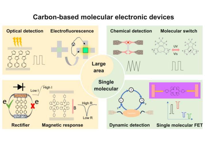
Molecule-based electronic devices, using the intrinsic electronic structure of molecules as device units and constructing electronic devices at the molecular scale, serve as an ideal experimental platform for studying molecular charge transfer mechanisms. They also provide a novel strategy for achieving new functional electronic devices at the micro-nano scale. The realization of a micro-nano electrode gap and a reliable electrode-molecule connection are key factors in developing highly reproducible molecular devices. Carbon materials have been widely applied in the construction of molecular devices due to their remarkable chemical stability and abundant surface chemistry. This review summarizes the research status of using carbon as electrodes in molecular device construction, showcasing the prominent advantages of carbon materials, such as high stability, low cost, and scalability, as well as their applications and research progress in large-area molecular devices and single-molecule devices. The review presents a wealth of achievements in the construction of functional molecular devices, such as molecular switches and rectifiers, using carbon electrodes, as well as the study of the structure-performance relationship in molecular-electron transport. Lastly, this work analyzes the challenges currently faced in carbon-based molecular device research and provides prospects for the chemical connection of carbon electrode-molecular interface and functionalization of carbon-based molecular devices, as well as the integration of future molecular devices.

Contents

1 Introduction

2 Electrode materials in molecular junctions

2.1 Metal electrodes

2.2 Semiconductor electrodes

2.3 Carbon electrodes

3 Carbon electrodes in large-area molecular devices

4 Carbon electrodes in single molecular junctions

4.1 Preparation technology of carbon-based single molecular junctions

4.2 Function and regulation of carbon-based single molecular junctions

4.3 Analysis and detection of carbon-based single molecule devices

5 Conclusion and outlook

Cite this article

Junhong Xue , Xuan Ji , Cong Chen , Xiaohai Ding , Xi Yu , Wenping Hu . Molecular Electronic Devices Based on Carbon Electrodes[J]. Progress in Chemistry, 2024 , 36(1) : 1 -17 . DOI: 10.7536/PC230618

1 Introduction

As silicon-based semiconductor device dimensions enter the sub-nanometer molecular level, quantum effects governing electronic behavior in devices begin to emerge, and Moore's law faces challenges[1]. However, the natural size of organic molecules is just in the nanometer range, and molecular electronic devices use a single or several organic molecules as the functional units of electronic circuits at the microscopic scale.It not only meets the growing demand for miniaturization of electronic devices, but also provides an ideal experimental platform for exploring the mechanism of cross-molecular charge transfer at the molecular level[2]. At the same time, the development of diverse functional electronic devices based on the regulation of molecular electrical properties by molecular design has attracted the research and attention of chemists[3~5]. Different from the traditional electronic circuit design logic, the research of molecular electronic devices combines the top-down microfabrication technology with the bottom-up molecular self-assembly method to realize the "electrode-molecule-electrode" device structure.The detection, conversion and storage of optical, electrical, magnetic, thermal, ionic, mechanical and chemical signals are realized at the molecular or supramolecular level, so as to prepare molecular-level electronic components with functions of switching, transistor, storage, light-emitting diode and rectification[6][7][8][9][10].
With the progress of micro-nano technology and material science, the preparation process of molecular electronic devices has also been fully developed. On the one hand, dynamic molecular junction forms based on Mechanically controllable break junction (MC-BJ), Scanning tunneling microscopy break junction (STM-BJ) and Scanning probe microscopy break junction (SPM-BJ) technologies have achieved the principle verification of functional devices with single molecules[11]. On the other hand, large area molecular electronic devices based on traditional chemical techniques such as Self-assembled monolayer (SAM), Langmuir-Blodgett (LB) film and electrochemical grafting have also been widely studied[12]. It is worth mentioning that the Canadian McCreery team has realized the commercial application of molecular devices in audio modification circuits[13]. At present, the field seems closer than ever to realizing the vision proposed by Aviram more than 40 years ago[14].
The fabrication process of molecular devices includes three main aspects: the selection of electrode materials, the treatment of electrode-molecule interface, and the design and synthesis of functional molecules[15]. Functional molecules are the main source of controlling charge transport and realizing device function; Electrode materials and electrode-molecule interface determine the charge injection barrier and interface electronic coupling strength of the device, which are important factors affecting the device performance, even dominating the device function[15,16]. The inherent high chemical stability, temperature stability, optical transparency, flexibility and abundant surface modification possibilities of carbon materials can not only effectively avoid the problems of electromigration and electrooxidation of metal electrodes,It can also meet the research and development needs of highly robust functional molecular devices, including optical coupling detection, magnetic field response, memristor and flexible electronic devices[11,17]. In this paper, the research status of using carbon materials as electrodes for molecular devices is reviewed, and the outstanding advantages of carbon materials in molecular device construction, such as high stability, low cost and mass production, as well as the application and research progress in large area molecular devices and single molecular junctions, are discussed. Finally, the current problems and future development directions of carbon-based molecular devices are analyzed, which provides a reference for the subsequent development of a variety of carbon-based functional devices and the construction of molecular circuits.

2 Structure and Electrode Materials of Molecular Electronic Devices

Molecular devices are "electrode-molecule-electrode" systems in which molecules are used as charge transport control units, and are mainly divided into two structures: single-molecule junctions (Figure 1A) and large-area molecular layer devices (Figure 1b). Among them, the single-molecule junction is connected to a single molecule through a micro-nano fabricated molecular scale electrode to form a control unit, which is the ultimate idea of device miniaturization. Molecular layer devices are constructed by combining single-layer (few-layer) molecular films with limited-scale electrodes with the help of mature molecular film preparation technology. Electrodes are the basic components of molecular electronic devices, which not only determine the preparation, structure and stability of molecular junctions, but also affect the charge transport behavior in junctions[15]. Therefore, the selection of electrode materials must take into account various factors, including chemical inertness, machinability, matching with organic molecules, molecule-electrode interface coupling, and the alignment of electrode and molecular orbital energy levels. From the material point of view, there are three kinds of electrode materials commonly used in the preparation of molecular electronic devices: metal electrode, semiconductor electrode and carbon electrode.
图1 (a) 单分子器件和 (b) 大面积分子器件的示意图

Fig. 1 Schematic diagram of a single molecule device (a) and a large area molecular device (b)

2.1 Metal electrode

Metal electrodes are the most commonly used electrodes. Noble metals, such as gold and platinum, which are chemically inert and easy to process, are usually used to prepare atomic-scale tip electrodes for single molecule devices or ultra-flat electrodes for molecular layer devices by different methods.
For single-molecule devices, the advantages of metal electrodes lie in their ductility and easy processability. Atomic-scale tip electrodes can be realized by electromigration and mechanical methods to capture single molecules for molecular devices[18~22]. Based on the clear charge transport pathway of the single-molecule device (Figure 2a), the researchers combined physical modeling and experimental data analysis to explore the charge transport mechanism (Figure 2b)[23~25]. On the other hand, metal electrodes have also been widely used in large area monolayer molecular devices[26]. In particular, SAM is formed on the surface of metals and metal oxides with thiol, carboxylic acid and other groups as adsorption groups. Due to the nature of coordination bonds or electrostatic adsorption between organic molecules and metal, molecules can spontaneously rearrange on the metal surface to form a dense and stable monolayer, which constitutes the basic structure of monolayer devices[27]. The molecular layer device can be constructed by covering the top electrode on it (Fig. 2C). In order to fabricate large area metal-top contact electrodes without damaging the active molecular layer, a variety of fabrication processes have been developed.Such as: curly gold nanomembranes, suspended nanowires, nano-printing transfer, lift-off and float (LOFO), photoreduced metal precursors, liquid metal (mercury and gallium-indium alloy (EGaIn)) and indirect thermal evaporation (introducing a buffer layer between the molecular layer and the metal electrode), etc[28][29][30][31][32][33][34][35,36].
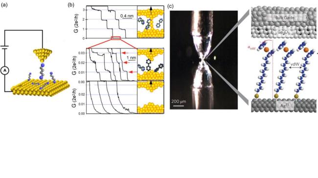
图2 (a) STM-BJ装置原理图;(b) STM-BJ测量过程示意图及相应的电导变化曲线[40];(c) 左:AgTS/SAM/Ga2O3/EGaIn分子结的光学显微镜图像;右:相应器件垂直结构示意图[41]

Fig. 2 (a) Schematic of STM-BJ set-up; (b) Schematic diagram of the STM-BJ measurement process and corresponding conductance change curves[40]. Copyright 2003, AAAS; (c) Left: optical microscope image of AgTS/SAM/Ga2O3/EGaIn molecular junctions (MJs); Right: vertical structure diagram of corresponding device[41]. Copyright 2013, Springer Nature

It should be pointed out that the metal electrode defects of molecular devices are also obvious. The electromigration, electrooxidation and mobility of metal atoms, as well as the unclear top electrode-interface introduced by the buffer layer addition process, will affect the mechanical stability and cycle test life of the device, and limit its practical application value.

2.2 Semiconductor electrode

Inspired by the traditional semiconductor device structure, silicon-based electrical large area molecular devices have also been widely concerned and explored. Different from Metal electrodes, Semiconductor electrodes have discontinuous electronic state distribution, and the electronic structure can be controlled by doping group III and V elements, so the device characteristics based on metal-molecule semiconductor (MmS) structure can show significant differences from those of metal-electrode molecular junctions[37~39]. On the one hand, the controllable rectification ratio of molecular devices can be achieved by adjusting the Fermi level of the electrode through the doping level of the semiconductor electrode[37]. On the other hand, although the depletion layer on the semiconductor side of the MmS device is the main cause of rectification, the active molecular layer, as a bridge for charge transport, can be treated by the interface chemical process to further adjust the actual rectification ratio in the device[42]. In addition, based on the photoresponse characteristics of semiconductors, Vezzoli et al. Achieved tunable photoresponse of molecular devices through physical doping and molecular engineering, which verified the application potential of high-sensitivity photocontrolled charge transport molecular devices[43].
Due to the charge rearrangement at the molecule-electrode interface caused by the molecular dipole, the charge transport at the molecule-electrode interface is dominated by the molecular structure, which makes the conductance of molecular devices have great differences in molecular characteristics. Haj-Yahia et al. achieved molecular control of device rectification performance by giving acceptor groups to regulate the molecule-electrode dipole direction (Fig. 3)[44]. Because semiconductor materials have a well-defined band gap between the valence band and the conduction band, the charge transport of MmS molecular junctions is more sensitive to the matching degree between the molecular energy level and the semiconductor band edge, thus showing a significant dependence of the molecular junction on the type of semiconductor carriers[45,46]. By covalently functionalizing semiconductor electrodes with organic molecules, novel molecular functions, such as molecular optical switching, charge storage, and biosensing, can be introduced into traditional semiconductor devices[47][48][49,50].
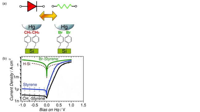
图3 (a) n-Si(111)/molecular/Hg分子整流器的示意图;(b) n-Si(111)/molecular/Hg分子结的J-V曲线(绿色:对溴代苯乙烯,蓝色:苯乙烯,黑色:对甲基苯乙烯)[44]

Fig. 3 (a) Schematic diagram of n-Si(111)/molecular/Hg molecular rectifier; (b) J-V curves for n-Si(111)/molecular/Hg molecular junctions (green: Br-styrene, blue: H-styrene, black: CH3-styrene) [44]. Copyright 2013, Wiley

2.3 Carbon electrode

Carbon electrodes, such as graphene, carbon nanotubes and high conductivity carbon films, have become another important material for the preparation of molecular devices in recent years because of their stable properties, high conductivity and low cost.
First of all, carbon materials have good conductivity, which can meet the needs of charge transport in molecular junctions. Table 1 lists the resistivity of several carbon materials. Although carbon thin film materials show a wide range of resistivity depending on the preparation conditions, their measured resistance is strongly dependent on the film geometry. For example, for a 1×1 cm2×100 nm thick carbon film with a resistivity of 0.15 Ω · cm, charge transport has a resistance of 15 kΩ in the in-plane direction and only a resistance of 10-5Ω in the direction perpendicular to the plane. Therefore, carbon materials are often used as molecular device electrodes, electrode buffer layers, or composite electrode materials.
表1 不同碳材料的相关物性比较

Table 1 Comparison of correlation properties of different carbon materials

Type of material Material density (g·cm-3) d002 (Å) ρ (Ω·cm) ref
HOPG, a-axis 2.26 3.354 4×10⁻⁵ 51
HOPG, c-axis 2.26 3.354 0.17 52
Disordered graphite 1.80 3.350 1×10⁻³ 53
Tokai GC-2000℃ 1.50 3.480 4.2×10⁻³ 54
Carbon fiber 1.80 3.400 (5~20)×10-4 55
Evaporation of amorphous carbon 2.00 >3.4000 ~103 56
Hydrogenated amorphous carbon 1.4~1.8 - 107~1016 57
PPF - - 0.006 58
B-doped diamond - - 0.05~0.5 59
Secondly, one of the advantages of carbon electrodes as alternative electrodes for molecular devices is that carbon electrodes are easily bonded by carbon-carbon covalent bonds (C — C: 4 eV; Au — S: 1.9 eV) forms stable and reliable chemical contacts with active molecules[60,61][62]. The gap electrode obtained by oxidation treatment of carbon nanotubes and graphene produces a carboxylic acid end, which can be covalently linked with amino derivative molecules through amide condensation reaction (Figure 4A), thus preparing a single molecule device with high mechanical stability. At the same time, because of its large conjugated structure, graphene carbon materials can make molecules with conjugated end groups form van der Waals contact with electrodes through π-π stacking (Fig. 4B), which greatly enriches the molecular species that can be used for single molecular junction construction[63,64]. In molecular layer devices, thanks to the excellent electrochemical activity of carbon electrode materials, the electrochemical reduction grafting method provides a rich surface modification strategy for carbon film electrodes (Figure 5A), so that molecules can be combined with the electrode through carbon-carbon covalent bonds (Figure 4C)[65]. Similarly, relying on the conjugated structure of layered graphene, large area molecular devices can also be fabricated by π-π stacking interaction with conjugated organic molecules (Fig. 4D)[63].
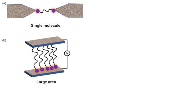
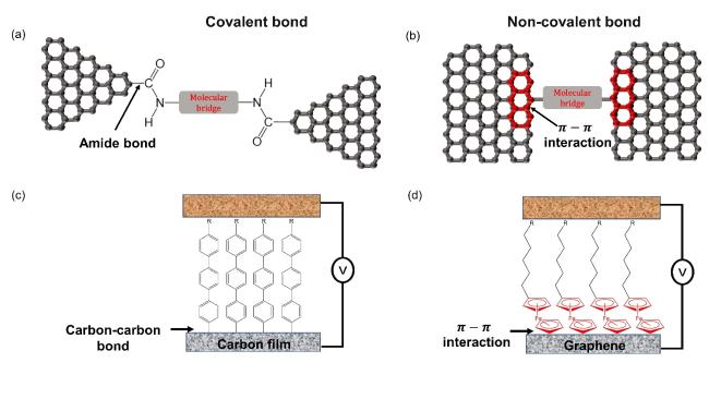
图4 (a) 通过共价酰胺键连接的单分子结示意图;(b) 通过π-π相互作用结合的单分子结示意图;(c) 通过碳碳共价键连接的大面积分子结示意图;(d) 通过π-π相互作用结合的大面积分子结示意图

Fig. 4 (a) Schematic diagram of a single molecular junction connected by a covalent amide bond; (b) Schematic diagram of a single molecular junction bound by π-π interaction; (c) Schematic diagram of large molecular junctions connected by carbon-carbon covalent bonds; (d) Schematic diagram of large molecular junctions bound by π-π interaction

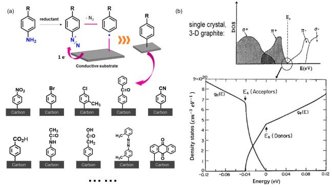
图5 (a) 上:芳香胺原位重氮化在碳电极表面接枝过程示意图[27],下:部分用于电接枝修饰碳表面的化学结构[65]; (b) 单晶石墨材料的态密度分布(下图为费米能级处态密度的放大图)[51]

Fig. 5 (a) Upper: Schematic diagram of the grafting process of the aromatic amine in situ diazotization on the surface of the carbon electrode[27]. Copyright 2020, MDPI, Basel, Switzerland; Lower: part representative chemical structure used for electrical grafting to modify carbon electrodes[65]. Copyright 2020, The Royal Society of Chemistry; (b) State density distribution of a single crystal graphite material (the figure on the right is an enlarged view of state density at the Fermi level) [51]. Copyright 2008, American Chemical Society

The Density of electron states (DOS) of electrode materials is also an important factor. DOS and its energy distribution affect the charge transfer rate between the electrode and the species, and also affect the voltage-current response characteristics and device function of the device. Unlike the high and flat DOS distribution of metal materials, the shape and size of DOS distribution of carbon materials vary greatly with their structure. For example, in highly oriented pyrolytic graphite (HOPG), the σ and π orbitals combine to form a filled valence band, shaded in fig. 5 B, while the antibonding orbital contains the conduction band. For infinite graphene and ideal graphite, the valence and conduction bands overlap at the Dirac point[54]. The DOS distribution of carbon nanotubes is related to their coil index and tube diameter, so carbon nanotube electrode materials have been widely used in the construction of single molecule devices because of their control space from metal to semiconductor. At the same time, the microcrystalline structure in the graphite lattice introduces many defect States between the conduction band and the valence band, so the electronic behavior of the carbon film electrode is similar to that of a metal with low DOS.
Finally, it is worth noting that devices constructed using carbon electrodes have good stability, taking carbon-based large area molecular devices as an example. Carbon films (electron beam evaporated carbon (eC) and pyrolytic photoresist film (PPF)) have sub-nanometer roughness, and the surface of carbon electrodes is easy to be chemically modified as mentioned above, so high-quality organic molecular films with rich molecular species and controllable thickness can be prepared on carbon electrodes to meet the needs of developing multi-functional molecular electronic devices. At the same time, unlike traditional graphite materials such as HOPG and polymer pyrolytic films, which usually require a graphitization process above 1000 ℃, Yan et al. Used eC materials with mild preparation conditions as the top electrode of the device, which can protect the molecular layer from the atomic penetration of the external metal wire, thus greatly improving the stability and yield of the device[66]. Compared with metal electrodes, carbon-based molecular devices used as top electrodes can withstand larger bias voltages, operate in a wider temperature range, and have long cycle life, which lays the foundation for building low-cost and practical molecular devices.

3 Carbon-based large area molecular device

In large area molecular devices, explicit molecule-electrode contacts are the structural basis for connecting theoretical calculation tools with experimental results, and also become a major challenge in the device construction process. Therefore, a variety of large area molecular device microfabrication schemes have been proposed at home and abroad, including liquid metal soft top contact, microchannel EGaIn contact electrode and the use of ultrafine contact area to reduce the irreversible damage to the molecular layer caused by thermal evaporation[33,67][68,69][70]. At the same time, the application of carbon electrodes in the fabrication of large area molecular devices has also attracted the attention of many researchers[15,17]. On the one hand, carbon materials (such as graphene, HOPG and eC) are ideal electrode materials for solid-state molecular devices because of their low resistance, flexibility, excellent optical transparency, low roughness and easy surface modification; On the other hand, carbon electrode materials are used to spacer/replace traditional metal electrodes to prepare molecular devices, which can avoid the destruction of molecular junctions caused by the migration of metal atoms at high current density, thus greatly improving the operation life of molecular devices and enabling molecular devices to work normally in a wider temperature range. In this section, the research progress of carbon materials in large-area molecular device structures is introduced from the aspects of large-area molecular junction construction, device charge transport mechanism and functionalization.
Conductive carbon materials have natural compatibility with organic molecules, and as the bottom electrode of molecular devices, they can realize a variety of contact modes, which ensures the universality of a variety of organic molecular structure-activity relationship studies. Sayed et al. Covalently combined conjugated molecules by electrochemical method. Due to the strong electrode-molecule coupling, the molecular energy level is seriously broadened, and the interface energy level arrangement deviates from the Schottky barrier model, resulting in compression effect[71]. Therefore, when the molecular thickness is less than 5 nm, that is, the molecular scale dominated by the tunneling mechanism, different conjugated molecules show similar conductivity characteristics and length dependence, and the molecular structure characteristics can not be highlighted. Nijhuis et al. Used the bottom electrode of graphene to connect with organic conjugated small molecules through π-π interaction to balance the molecule-electrode coupling strength, and realized a molecular diode device with high rectification characteristics based on a single molecular layer[63].
Due to the easy processability and structural rigidity of carbon materials, they have more advantages in the top contact electrode application of large area molecular devices. In 2012, Laursen et al. Used the reduced graphene oxide film treated by low-cost solution method as the top contact of molecular devices to achieve 90% device yield, but this method involves high temperature treatment and complex process[72]. In order to simplify the preparation process, graphene oxide was directly used as the top contact of SAM devices in 2018, and it was found that its interface resistance was comparable to that of graphene top contact devices, which provided a new way to design a new generation of molecular solid-state devices[73]. In addition to graphene, commercial carbon paste is also used as a molecular junction top contact buffer layer. In 2020, Nijhuis group used carbon paste with high metal-like conductivity as the buffer layer of SAM device by spin coating method[74]. Because the work function of carbon paste is close to that of gold electrodes, they obtained high-quality large-area molecular junctions with ultra-low contact resistance, and the good fluidity of carbon paste materials solved the problem of unclear effective area of charge transport caused by interface roughness.
McCreery's team has fully developed a process for preparing molecular thin film devices based on the combination of amorphous carbon and electrochemical grafting growth of molecular layers (Figure 6)[62]. They used patternable eC electrode materials and introduced molecular active layers by electrochemical reduction of aryl diazonium salts to prepare cruciform molecular junctions. The fabrication of this molecular device can be extended to wafer size, and the device can be integrated (Figure 7 a), which is compatible with traditional metal oxide semiconductor device fabrication technologies[59]. It should be pointed out that the use of carbon-based materials instead of traditional metal electrode materials for direct contact not only ensures the high yield of devices, but also has long cycle operation stability and good device life[59,66]. For example, Bergren et al. Reported a molecular junction electronic device based on the covalent connection of PPF and eC, and they used the nonlinear tunneling current feedback of carbon-based molecular devices as the limiting element of the electric guitar.It is found that the distribution of odd and even harmonics of electric guitar sound output can be changed, and then the output sound wave is softer than that of the traditional diode limiting element, so as to achieve excellent moistening effect[13]. It is worth noting that the electrical properties of molecular junctions can be changed by molecular species and molecular layer thickness, so continuous audio modification can be achieved through different molecular device combinations, which has been commercialized, and this work has greatly inspired the majority of molecular device development practitioners.
图6 基于电子束沉积碳和电接枝法制备大面积分子器件流程示意图[62]

Fig. 6 Schematic diagram of large area molecular devices prepared by electron beam deposited carbon and electrografting[62]. Copyright 2010, American Chemical Society

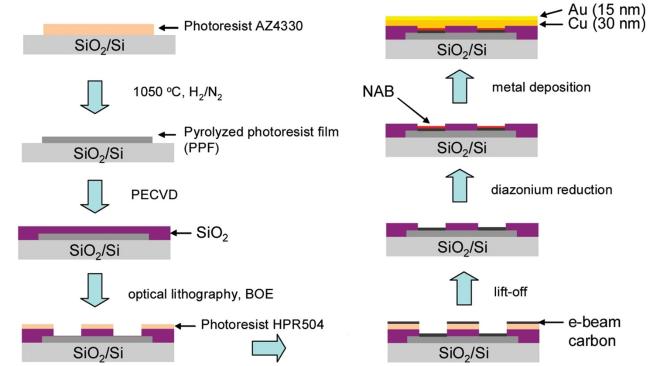
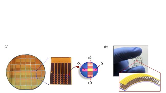
图7 (a) 在直径100 mm晶圆上基于eC和电接枝制备的碳基分子电子芯片光学图像以及其局部放大分子结的示意图;(b) 柔性衬底上碳基器件的弯曲光学图像及单个分子结弯曲状态下的结构示意图[59]

Fig.7 (a) Optical image of a carbon-based molecular electronic chip prepared by eC and electrical grafting on a 100 mm diameter wafer and schematic diagram of its locally amplified molecular junction; (b) Bending optical image of a carbon-based device on a flexible substrate and schematic diagram of a single molecular junction in bending state[59]. Copyright 2016, American Chemical Society

In addition, due to the translucency and flexibility of carbon materials, they can be deposited on a suitable substrate to achieve in-situ spectral detection or to prepare flexible molecular devices. As shown in Figure 7B, a crisscross molecular junction is prepared on a PET plastic substrate, and the device has good flexibility and can work normally in a bent state[75][59]. Moreover, in recent years, due to the above advantages of carbon materials, the preparation process of carbon-based devices has developed rapidly, and the study of charge transport mechanism using carbon-based molecular scale device research platform has also made important progress.
By introducing conjugated and complex structure molecules, Tefashe et al. Have a difference in device conductance of up to 7 orders of magnitude[75]. The introduction of metal ions makes the molecular optical gap smaller, the HOMO level close to the Fermi level of the carbon electrode, and the molecule-electrode interface mixed-valence electron configuration leads to a weak length dependence of the molecular conductance, which provides a basis for the design of long-range charge transport structures. The above conclusion is consistent with the experimental results of gold electrode large area molecular device and single molecule device, which proves the unification of different experimental platforms such as single molecule junction and large area molecular layer device in the study of charge transport mechanism[76][23]. Carbon-based large-area molecular junctions can well reflect the molecular characteristics and have superior stability, which makes it possible to customize the function of carbon-based molecular devices through molecular design. Barraud et al. Fabricated a C/1- (2-bisthienyl) -4-aminobenzene (BTB)/Ti/Au large area molecular device using carbon electrodes, which achieved a rectification ratio of 100 at a bias voltage of 2 V[77]. The asymmetric charge transport is due to the energy level pinning effect at the top contact interface of the metal electrode, and the carbon electrode-molecule covalent connection ensures the efficient charge injection. On the contrary, there is no rectification phenomenon in the device with C/BTB/C symmetrical electrodes constructed by the same BTB molecule[78]. Based on the PN junction structure, Bayat et al. Used continuous electrochemical deposition to prepare carbon-based bilayers to achieve the rectification function, and the energy level difference of the bilayers and the deposition sequence can determine the rectification scale and direction, respectively[79].
Carbon film electrodes have good optical transparency and are often used in the study of optical coupling of solid-state molecular devices. Najarian et al. constructed an optically transparent all-carbon molecular device on a quartz substrate (Fig. 8B), and used the measurement setup shown in Fig. 8A to study the photoresponse mechanism in devices based on different aromatic molecules[80]. The results show that the photocurrent and open-circuit voltage (Fig. 8C) generated by the device under illumination are inversely proportional to the molecular optical gap, and the polarity of the photocurrent and open-circuit voltage depends on the relative position of the molecular frontier orbital and the Fermi level of the electrode. In addition, the threshold bias for photocurrent generation reflects the interface barrier correlation, and the lower the threshold, the larger the coupling strength. In order to further study the mechanism of intermolecular long-range charge transport when the molecular layer exceeds the typical tunneling scale, Saxena et al. Used nitroazobenzene molecules and found that although the photocurrent is several orders of magnitude higher than the dark current, the length dependence of the two is consistent and the activation energy barrier is lower[81]. That is to say, the photocurrent depends on the multi-step tunneling process between adjacent molecules, while the dark current is limited by the charge interface injection, which provides a reliable design strategy for the design of photoresponsive molecular devices and long-range charge transport molecular structures.
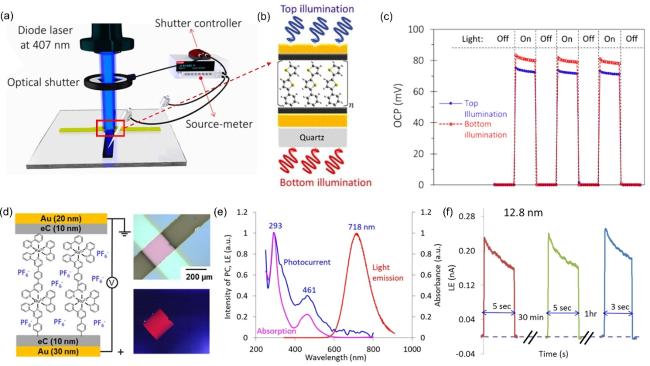
图8 (a) 开路电势(OCP)测量装置示意图;(b) BTB分子结示意图(底部:石英,顶部:碳);(c) 观察407 nm二极管激光上下照射BTB分子结三个开/关光周期的OCP[80];(d) Au/eC/Ru(bpy)3/eC/Au分子器件示意图及其施加电压前后分子结的光学图像;(e) Ru(bpy)3(12.8 nm)分子结的紫外吸收、光电流和发光光谱叠加图;(f) Ru(bpy)3(12.8 nm)分子结在乙腈蒸气下,3.2 V的偏置脉冲和静置几分钟的MJ重复脉冲的总光发射与时间的关系[9]

Fig. 8 (a) Schematic diagram of OCP measuring apparatus; (b) Schematic diagram of BTB MJ (Bottom: quartz, top: carbon); (c) Observed OCP for three on/off light cycles for BTB MJ with top and bottom illumination by a 407 nm diode laser[80]. Copyright 2018, American Chemical Society; (d) Schematic diagram of Au/eC/Ru(bpy)3/eC/Au molecular junction and optical image of molecular junction before and after voltage application; (e) Overlay of UV absorption, photocurrent and luminescence spectra of Ru(bpy)3(12.8 nm) MJs; (f) Total light emission versus time under acetonitrile vapor for bias pulses of 3.2 V and repeated pulses for Ru(bpy)3(12.8 nm) MJ at rest for several minutes after a bias pulse[9]. Copyright 2019, American Chemical Society

The transparency of carbon film electrode can not only realize the study of photoelectric coupling, but also carbon-based molecular devices can realize the function of molecular luminescence through molecular engineering, similar to organic light-emitting diodes and cascade laser devices. Ivashenko et al. Observed light emission in a wide wavelength range in conjugated small molecule devices. Compared with alumina tunnel junction, they found that the luminescence came from the radiative transition process of emitter electrons passing through the molecular layer to the collector, and the difference between the maximum emission photon energy and the emission electron energy was the energy loss of the molecular layer[82]. This provides a feasible scheme for identifying the charge transport mechanism in molecular devices. They further studied the Ru(bpy)3 molecule based on the luminescent material bipyridine ruthenium complex (Fig. 8d), and observed the luminescence phenomenon with molecular characteristics (Fig. 8e)[83]. Unlike organic light-emitting diodes, the device has no selectivity to voltage polarity, and the emission intensity depends on the bias voltage. The molecular device's luminescence delay of less than 5 ms and sustained luminescence lifetime of more than 10 H provide an experimental example for molecular optoelectronic devices (Figure 8 f). Further study shows that the threshold voltage of luminescence corresponds to the molecular optical gap, that is, bipolar injection from both electrodes forms Ru1+ and Ru3+, and excited state Ru2+ is formed in the middle of recombination, which relaxes luminescence[9]. This enables the fabrication of high-efficiency light-emitting molecular devices with symmetric electrodes and without transport layers.
Low temperature environment can avoid the interference of thermal fluctuations on the study of weak interactions. Due to the excellent temperature stability of carbon materials, carbon-based molecular devices can achieve ultra-low temperature multi-physical field testing. Yu et al. found the magnetoresistance effect with molecular characteristics based on the redox-active Ru(tpy)2 carbon electrode molecular device, and attributed the magnetoresistance effect to the bipolaron transport contribution through the sensitivity analysis of charge transport distance, temperature, bias and other systems (Fig. 9a)[84]. That is to say, organic molecules have large charge transfer reorganization energy, which reduces the effective charging energy of molecules and is conducive to the formation of ground States with even electrons. During multiple charge transport encounters, the bipolaron formation probability is modulated by the external magnetic field due to the spin blockade mechanism of the two-electron occupied state, thereby exhibiting a significant magnetic field-dependent resistance change of the molecular device at low temperatures (Fig. 9b). This study reveals the multi-particle transport mechanism in molecular electronic devices, and provides a reliable theoretical basis for the application of molecular scale devices in spin and magnetic functions through molecular design.
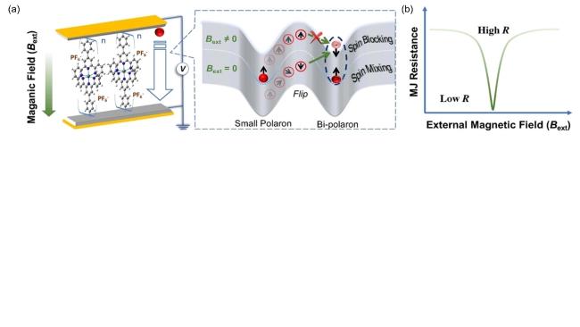
图9 (a)左:Au/a-C/Ru(tpy)2/a-C/Au分子结的示意图,右:分子结内双极化子电荷输运机理示意图(a-C:无定形碳膜);(b) Au/a-C/Ru(tpy)2/a-C/Au分子结的磁响应曲线[84]

Fig. 9 (a) Left: Schematic diagram of the Au/a-C/Ru(tpy)2/a-C/Au molecular junctions, Right: schematic diagram of charge transport mechanism of bipolaron in molecular junction(a-C: amorphous carbon film); (b) Magnetic response curve of Au/a-C/Ru(tpy)2/a-C/Au molecular junction[84]. Copyright 2022, Wiley

4 Carbon electrode single molecule device

Single-molecule devices are a reliable platform to explore the mechanism of intramolecular charge transport, and also create the possibility of further miniaturization of devices. Due to the advantages of carbon materials mentioned above, carbon-based single molecule devices have attracted the attention of many scientists from different disciplines in the past decades, and researchers have tried to replace metal electrodes with carbon electrodes (such as single-walled carbon nanotubes (SWNTs) and graphene)[51,85 ~88][11,89]. In this section, the main preparation methods of carbon nanoelectrodes and the typical research results of functionalized single molecule devices are reviewed.

4.1 Carbon based monomolecular junction fabrication technique

With the continuous development of the preparation process of carbon nanotubes and graphene materials, carbon materials with high conductivity and good stability (thermal, mechanical and chemical) are widely used in the development of single-molecule devices. At present, the preparation process of nanogap carbon electrode is relatively mature. For example, in 2010, Krupke et al. Successfully obtained a stable and controllable carbon nanotube electrode for the construction of single molecule devices by feedback electrosintering (Figure 10a)[93]. However, the carbon nanotube electrode prepared in this way mainly relies on π-π interaction to form a connection with organic molecules, resulting in insufficient stability of the single molecule junction. Guo et al. prepared a carboxylic acid-functionalized carbon nanotube electrode with a molecular-scale gap (< 10 nm) by precise oxidative cutting with a photolithographic mask (Fig. 10B), and covalently bonded amino derivative molecules to carbon nanotubes through amide condensation reaction to form a highly stable single-molecule device[94][87]. Similarly, carbon nanotube electrodes with controllable gaps can also be prepared by tunable ion beam current and focused ion beam dose (fig. 10 C)[95]. In addition, zigzag graphene electrodes are popular with researchers because they can provide clear molecular connection sites. In 2011, Prins et al. successfully constructed a "graphene-monomolecule-graphene" device (Fig. 10d) by preparing several layers of graphene electrodes with nanogaps using a controllable electrical burning method, and achieving conjugated connection through π-π stacking between conjugated molecules and the end of the electrode[64]. In order to realize the rigid connection between electrode and molecule, Guo Xuefeng et al. Used oxygen plasma etching method to prepare nanoscale gap graphene electrode with carboxyl terminal, and prepared covalent bonding single molecule junction based on amide condensation, which significantly improved the measurement stability of single molecule device[11][95]. The development of this technology has also brought the research of single-molecule electronics into a new era (Figure 10E). In recent years, based on the development of MC-BJ, organic functional molecules are placed between two graphene layers sliding with each other, and the preparation of layer-by-layer stacked graphene/molecule/graphene single-molecule devices has also been developed[92,96,97]. In 2019, Hong Wenjing et al. Prepared a series of all-carbon single-molecule junction systems with a size of only about 1 nm based on the MC-BJ technology of graphene electrodes (Fig. 10f), which experimentally proved that different fullerenes could be used to adjust the energy band of the device.So as to realize the conductance regulation of more than one order of magnitude, which is of great significance to the development of all-carbon electronics and is expected to become the core material and device of the next generation of carbon-based chip technology[92].
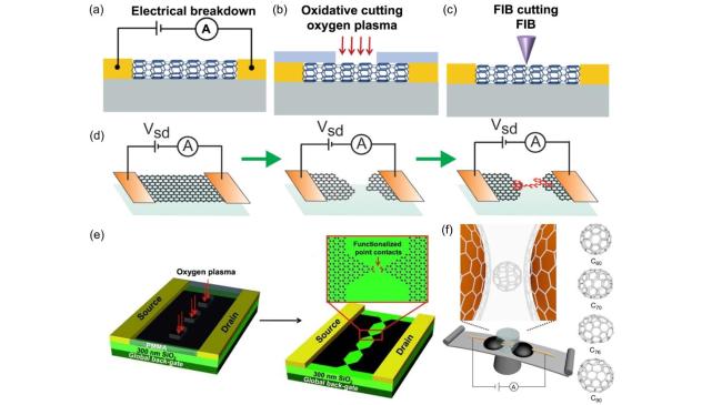
图10 制备碳纳米管纳米电极示意图[90]:(a) 电烧结法;(b) 氧等离子体氧化切割法;(c) 聚焦电子束切割法;(d) 电烧结法制备石墨烯纳米电极示意图[64];(e) 锯齿状石墨烯点接触阵列的制备,左:氧等离子体通过电子束光刻定义的锯齿状PMMA窗口精确切割石墨烯片的示意图,右:通过氧化切割形成的锯齿状石墨烯触点被羧酸端基功能化并且分离仅有几纳米的示意图[91];(f) 机械控制断结和石墨烯/单富勒烯/石墨烯结示意图以及C60、C70、C76和C90的化学结构[92]

Fig. 10 Schematic diagram of preparing carbon nanotube nanoelectrodes[90]. Copyright 2022, IOP Publishing. (a) Electrical breakdown method; (b) Oxygen plasma oxidation cutting method; (c) Focused electron beam cutting; (d) Schematic diagram of preparation of graphene nanoelectrodes by Electrical breakdown [64]. Copyright 2011, American Chemical Society; (e) Fabrication of indented graphene point contact arrays. Left: schematic illustration of an oxygen plasma precisely cutting a graphene sheets through an indented PMMA window defined by electron-beam lithography. Right: schematic illustration of indented graphene point contacts formed by oxidative cutting were functionalized by carboxylic acid end groups and separated by as little as a few nanometres. [91]. Copyright 2012, Wiley; (f) Schematic of mechanically controlled break junction and graphene/single-fullerene/graphene junction and chemical structure of C60, C70, C76, and C90[92]. Copyright 2019, Springer Nature

4.2 Function and Regulation of Carbon-based Single Molecule Devices

The controllable regulation of charge transport in molecular junctions can be achieved by external stimuli such as illumination, magnetic field and electric field, and then a variety of single-molecule functional devices such as controllable switches and high-performance field effect transistors can be fabricated. Molecular isomerization is well known to achieve conductance-responsive switching. However, how to achieve a stable and reproducible conductance switch at the single molecule level has been puzzling researchers for a certain period of time. It is generally believed that the strong coupling between the molecular active center and the electrode leads to the inhibition of molecular isomerization. To solve this problem, Guo Xuefeng et al. Used the above highly stable graphene electrode with carboxylic acid terminal combined with diarylethene amidation reaction to achieve stable, reliable and repeatable photocontrolled conductivity switching at the single molecule level for the first time through methylene decoupling[89]. As shown in fig. 11A, the diarylene molecule can be reversibly switched in both open and closed modes under UV-Vis light irradiation, thereby realizing the controllable switching of the device conductance between high and low States (fig. 11b). Based on graphene electrodes, they also developed a single-molecule reversible conductance switch that can trigger the isomerization of azobenzene molecules both under illumination and under electric field stimulation[98]. In addition, in 2022, based on the carbon nanotube electrode with the same high stability, Lee et al. Successfully fabricated a ferroelectric memory device with 1 nm2, ultra-small area and high operation stability (300 cycles) by using the isomerization reaction of azobenzene induced by electric field (Fig. 11c)[99]. As shown in Figure 11D, the azobenzene molecule creates a huge memory window of about 5 orders of magnitude (Vds=5 V) when it is switched between cis-trans configurations under electric field driving.
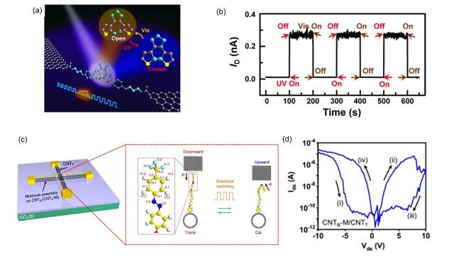
图 11 (a) 石墨烯-二芳基乙烯-石墨烯结的示意图;(b) 紫外可见光辐射下,二芳基乙烯分子在打开和关闭形式下可逆切换引起的实时测量电流,VD =100 mV,VG =0 V[89];(c) 左:CNTB-M/CNTT vdWI器件的三维图,右:依据电场开关CNTB-M/CNTT vdWI中基于反式和顺式异构体的分子极化变化的DFT模拟模型;(d) CNTB-M/CNTT vdWI器件的Ids-Vds曲线(分子在顺反状态间切换产生存储窗口)[99]

Fig.11 (a) Schematic diagram of a graphene-diarylethene-graphene junction; (b) Real-time measurement of the current through a diarylethene molecule that reversibly switches between the closed and open forms, upon exposure to UV and Vis radiation, respectively. VD =100 mV and VG =0 V[89]. Copyright 2016, AAAS; (c) Left: three-dimensional view of the CNTB-M/CNTT vdWI device, Right: DFT simulation model of the molecule polarization change based on trans and cis isomers in CNTB-M/CNTT vdWI according to electrical switching. (d) Ids-Vds curves of CNTB-M/CNTT vdWI device (the switching of molecules between trans and cis states leads to the generation of a memory window)[99]. Copyright 2022, Springer Nature

The single molecule device with graphene electrode has a planar structure, which is convenient for gate gating by various means, and can be used to construct a multifunctional single molecule field effect transistor. In 2018, Xin et al. Fabricated single-molecule junctions based on aromatic ring molecules on graphene electrodes, and used ionic liquids as gate electrolytes to construct field effect transistors[100]. It is found that changing the gate voltage can effectively adjust the alignment between the molecular frontier orbital and the Fermi level of graphene, thus realizing bipolar charge transport in electrochemically inert molecular systems, which provides a new way to develop high-performance single-molecule electrochemical transistor devices. Based on the versatility of organic molecules, in 2022, Yan et al. prepared a bifunctional field effect transistor based on a single porphyrin molecule, using ionic liquid gate control (Figure 12A) to achieve more than three orders of magnitude of conductance control (Figure 12c)[101]. In addition, in the switching mode, the porphyrin molecule can be induced to undergo reversible proton transfer isomerization by applying a bias, resulting in a double or quadruple jump in conductivity (Figure 12 B), which provides new possibilities for the realization of single-molecule logic gates, memories, and sensors. Different from the above device construction methods, based on the layered planar structure of graphene electrodes, Yang et al. Recently reported a single-molecule two-dimensional van der Waals heterojunction (Fig. 12d) with graphene-molecule-graphene structure constructed by layer-by-layer stacking, forming cross-plane charge transport.The conductance of the device changes with the electric field intensity by stimulating the conformational transition of a single molecule with an electric field (Fig. 12e), based on which a field-controlled reversible molecular switch is obtained by controlling the voltage across the molecular junction between 100 mV and 300 mV (Fig. 12f)[97].
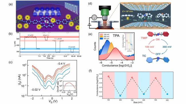
图 12 (a) 石墨烯-卟啉-石墨烯结示意图,突出离子液体门控和氢互变异构;(b) 通过卟啉分子的实时电流测量,在VD=950 mV时,四个态之间的转变;(c) 在VD= -0.02、-0.1、-0.2、-0.3和-0.4 V下器件的转移特性(插图展示了偏压依赖的开关比)[101];(d) 跨平面断裂结装置和外加电场作用下3个M-2D-vdWHs分子结内构象演变示意图;(e) 左:TPA M-2D-vdWHs分别在100、200和300 mV偏压下的1D电导直方图,插图给出了典型的电导-位移轨迹;右:TPA随电场的演变示意图,从具有高电导率的TWP构象(ON状态)到具有低电导率的TC构象(OFF状态);(f) 电场在100和300 mV之间切换时TPA M-2D-vdWHs的可逆开关[97]

Fig. 12 (a) Schematic of a graphene-porphyrin-graphene junction that highlights ionic liquid gating and hydrogen tautomerization; (b) Real-time measurement of the current through a porphyrin molecule that highlights the transitions between four states at 950 mV; (c) Transfer characteristics at VD= -0.02, -0.1, -0.2, -0.3, and -0.4 V (Inset shows VD-dependent on/off ratios)[101]. Copyright 2022, AAAS; (d) Schematic diagram of the XP-BJ setup and the conformational evolution of three M-2D-vdWHs under the applied electric field; (e) Left: The 1D conductance histograms for TPA M-2D-vdWHs under the bias of 100, 200, and 300 mV, respectively. The inserts give the typical conductance-displacement traces, Right: Schematic evolution of TPA along with the electric field, from a TWP conformation with a high conductivity (ON state) to a TC conformation with a low conductivity (OFF state); (f) Reversible switching of TPA M-2D-vdWHs as the electric field was switched between 100 and 300 mV[97]. Copyright 2023, AAAS

4.3 Carbon-based single-molecule device analysis and detection

The chemical stability of carbon materials ensures that carbon-based single-molecule devices have a certain tolerance under different chemical environments and voltage stimuli, which makes single-molecule detection possible. Moreover, based on the measurement at the single molecule level, the detection sensitivity is higher[102]. Combining molecular electronics with biological systems, in 2007, Nuckolls et al. Connected functionalized molecules between carbon nanotubes, and realized directional recognition for bioelectric detection by means of specific assembly between probes and biomolecules[103]. Based on this principle, they constructed a functionalized single-molecule device using DNA aptamer molecules with G4 conformation, which achieved highly selective and sensitive reversible detection of thrombin (Fig. 13)[104]. In 2011, Shionoya et al. Introduced unnatural base pairs containing metal ions into DNA strands, and the reversible control of conductance switch function could be achieved by alternating treatment of chelating reagent EDTA and metal ions[88]. In 2012, Cao et al. Also observed a similar reversible switching effect based on terpyridine molecules using graphene as electrodes. Based on this electrical property, they realized the high-sensitivity detection of metal ions at the single molecule level[91]. In addition to the above, the single-molecule device can also be used for pH detection. In 2006, Guo et al. Realized the reversible molecular switch of acid-base regulation by using the protonation and deprotonation reaction of polyaniline monomolecular junction, which was used for the electrical detection of solution pH[94]. In a word, carbon-based single-molecule devices can convert chemical reactions or biospecific recognition into electrical signals, and realize real-time visual monitoring of organism characteristics.
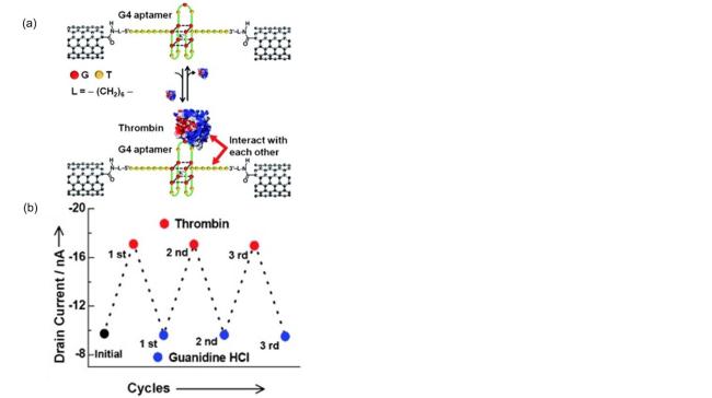
图 13 (a) 单分子器件在单分子水平上检测蛋白质的传感机制示意图;(b) 当凝血酶和盐酸胍交替处理时,同一器件的三个代表性开关周期,VSD = -50 mV[104]

Fig. 13 (a) Schematic representation of the sensing mechanism showing single-molecule devices detect proteins at the single-molecule level; (b) Three representative switching cycles for the same device when alternately treated with thrombin and guanidine HCl, VSD = -50 mV[104]. Copyright 2011, Wiley

Single-molecule devices can not only facilitate the miniaturization of electronic devices, but also serve as a research tool to probe quantum transport properties and as a high-resolution single-molecule platform to study the microscopic dynamics of various chemical and physical behaviors[96,105]. In recent years, Xuefeng Guo et al. Have developed a novel label-free single-molecule detection strategy, which uses stable graphene-single-molecule devices to directly explore the dynamic process of basic chemical reactions, reveal the time trajectories and reaction paths of various intermediates and even transition States, and expand to various important chemical reaction fields, such as photocatalysis and electrocatalysis. In 2018, based on a single molecular junction containing a 9-fluorenone center, Guan et al. Monitored in situ two different conductance signals oscillating on a microsecond time scale in a hydroxylamine solution environment, and explained the reversible transition between the reactant and the intermediate state in the nucleophilic addition process of NH2OH and carbonyl by combining with theoretical simulation[107]. This method provides a novel, sensitive and high spatiotemporal resolution technique for the study of unimolecular hydrolysis reactions.
At the same time, carbon-based single-molecule devices can also be used to study molecular interaction dynamics. Guan et al. Used carbon-based single-molecule devices to achieve real-time monitoring of single-molecule hydrogen bond dynamics with single-bond scale resolution.The mechanism of structural change of a single molecule containing four hydrogen bonds by proton transfer and lactam-lactam isomerization under the action of an electric field is revealed, which provides a new perspective for understanding the role of hydrogen bonds in various processes[108][107]. Based on this, they further combined molecular engineering with single-molecule detection, opening up a new way to explore the reaction mechanism at the molecular level. In 2021, Yang et al. Covalently embedded a single palladium catalyst into a graphene nanogap, directly probed the complete catalytic cycle of the Suzuki-Miyaura coupling reaction (Figure 14 a) using an ultra-high time resolution single-molecule platform, and clarified the ligand-exchange preferential pathway of the reaction[106]. At the same time, they also determined the thermodynamic and kinetic information of each basic reaction step (Figure 14B), as well as the Suzuki-Miyaura coupled overall catalytic time scale. Recently, Zhang et al. Realized the precise control of Mizoroki-Heck reaction pathway by gate voltage based on single-molecule devices, and deciphered its detailed internal mechanism based on electrical detection, helping chemists to precisely adjust chemical reactions in a predictable and controllable manner[109].
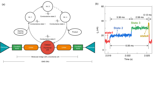
图14 (a)监测单分子催化循环过程的策略及其器件结构的示意图,在电流中可以检测到催化功能中心的实时变化;(b) 通过催化功能中心的实时变化能够在电流中被检测,突出强调一个催化循环过程中四个导电态的转变[106]

Fig.14 (a) Schematic strategy of the monitoring process for a single-molecule catalytic cycle and device structure; (b) Real-time measurement of the current through catalyst functional unit that highlights the transitions between four conductance states of one catalytic cycle[106]. Copyright 2021, Springer Nature

5 Conclusion and prospect

Unlike traditional microelectronic devices, which rely on the bulk and interface properties of materials, molecular electronic devices can realize the regulation of charge transport from nanoscale organic basic units. In recent years, with the joint efforts of researchers in chemistry, physics, microelectronics and many other fields, gratifying achievements have been made in the construction of stable devices, the study of charge transport mechanism and the exploration of device functionalization. In this paper, we focus on the electrode materials of molecular electronic devices, briefly summarize the common electrode materials and their construction methods, and focus on the advantages of carbon materials as molecular electronic devices and the research results in related fields. Although carbon-based molecular devices have made remarkable progress, they still face many challenges and opportunities. First of all, due to the high chemical stability of carbon materials, the field of molecular devices mainly relies on amide condensation and electrochemical diazonium salt reduction to achieve covalent contact of molecular junctions. The development of new controllable chemical reactions at the carbon electrode interface is an important aspect of the preparation of molecular devices based on carbon electrodes. The use of abundant organic reactions, such as metal-catalyzed carbon-carbon coupling, will create abundant possibilities and provide opportunities for new molecular functional devices. Secondly, the abundant allotropes of carbon materials make them present a variety of optoelectronic properties, which can be fully combined with the optoelectronic properties of carbon electrodes to achieve new device functions, which is also an important direction for the future development of molecular electronics. Thirdly, at present, the research of carbon-based molecular devices is still limited to the development of single device functions, and the realization of complex logic functions through device combination and integration to promote the development of single molecular integrated circuits will be the only way for single molecular devices to move towards large-scale applications (Figure 15). Stable carbon electrode single molecule devices have laid the foundation for this process, and the future can be expected.
图15 基于碳电极的分子尺度电子器件发展展望概念图

Fig. 15 Prospect concept map of molecular scale electronic devices based on carbon electrode.

[1]
Waldrop M M. Nature, 2016, 530(7589): 144.

[2]
Xiang D, Wang X, Jia C, Lee T, Guo X. Chem. Rev., 2016, 116(7): 4318.

[3]
Klyamer D D, Sukhikh A S, Krasnov P O, Gromilov S A, Morozova N B, Basova T V. Appl. Surf. Sci., 2016, 372: 79.

[4]
Kumari A, Dhawan S, Singh H, Haridas V, Sinha A. J. Mol. Liq., 2022, 359.

[5]
Guzel M, Torlak Y, Choi H, Ak M. Eur. Polym. J., 2023, 186.

[6]
Hnid I, Frath D, Lafolet F, Sun X N, Lacroix J C. J. Am. Chem. Soc., 2020, 142(17): 7732.

[7]
Xin N, Hu C, Al Sabea H, Zhang M, Zhou C, Meng L, Jia C, Gong Y, Li Y, Ke G, He X, Selvanathan P, Norel L, Ratner M A, Liu Z, Xiao S, Rigaut S, Guo H, Guo X. J. Am. Chem. Soc., 2021, 143(49): 20811.

[8]
Li J, Hou S, Yao Y R, Zhang C, Wu Q, Wang H C, Zhang H, Liu X, Tang C, Wei M, Xu W, Wang Y, Zheng J, Pan Z, Kang L, Liu J, Shi J, Yang Y, Lambert C J, Xie S Y, Hong W. Nat. Mater., 2022, 21(8): 917.

[9]
Tefashe U M, Van Dyck C, Saxena S K, Lacroix J C, McCreery R L. J. Phys. Chem. C, 2019, 123(48): 29162.

[10]
Chen X P, Roemer M, Yuan L, Du W, Thompson D, del Barco E, Nijhuis C A. Nat. Nanotechnol., 2017, 12(8): 797.

[11]
Yang C, Yang C, Guo Y, Feng J, Guo X F. Nat. Protoc., 2023, 18(6): 1958.

[12]
Gorenskaia E, Turner K L, Martin S, Cea P, Low P J. Nanoscale, 2021, 13(20): 9055.

[13]
Bergren A J, Zeer-Wanklyn L, Semple M, Pekas N, Szeto B, McCreery R L. J. Phys. Condens. Matter, 2016, 28(9): 094011.

[14]
Aviram A, Ratner M A. Chem. Phys. Lett., 1974, 29(2): 277.

[15]
Xin N, Guan J, Zhou C, Chen X, Gu C, Li Y, Ratner M A, Nitzan A, Stoddart J F, Guo X. Nat. Rev. Phys., 2019, 1(3): 211.

[16]
Li X, Ge W, Guo S, Bai J, Hong W. Angew. Chem. Int. Ed., 2023, 62(13): e202216819.

[17]
McCreery R L. Acc. Chem. Res., 2022, 55(19): 2766.

[18]
Park H, Lim A K L, Alivisatos A P, Park J, McEuen P L. Appl. Phys. Lett., 1999, 75(2): 301.

[19]
Reed M A, Zhou C, Muller C J, Burgin T P, Tour J M. Science, 1997, 278(5336): 252.

[20]
Bai J, Daaoub A, Sangtarash S, Li X, Tang Y, Zou Q, Sadeghi H, Liu S, Huang X, Tan Z, Liu J, Yang Y, Shi J, Meszaros G, Chen W, Lambert C, Hong W. Nat. Mater., 2019, 18(4): 364.

[21]
Huang X, Tang C, Li J, Chen L C, Zheng J, Zhang P, Le J, Li R, Li X, Liu J, Yang Y, Shi J, Chen Z, Bai M, Zhang H L, Xia H, Cheng J, Tian Z Q, Hong W. Sci. Adv., 2019, 5(6): eaaw3072.

[22]
Bumm L A, Arnold J J, Cygan M T, Dunbar T D, Burgin T P, Jones L, Allara D L, Tour J M, Weiss P S. Science, 1996, 271(5256): 1705.

[23]
Yao X L, Sun X N, Lafolet F, Lacroix J C. Nano Lett., 2020, 20(9): 6899.

[24]
Luo L, Benameur A, Brignou P, Choi S H, Rigaut S, Frisbie C D. J. Phys. Chem. C, 2011, 115(40): 19955.

[25]
Yao X, Vonesch M, Combes M, Weiss J, Sun X, Lacroix J C. Nano Lett., 2021, 21(15): 6540.

[26]
Jeong H, Kim D, Xiang D, Lee T. ACS Nano, 2017, 11(7): 6511.

[27]
Herrer L, Martin S, Cea P. Appl. Sci. Basel, 2020, 10(17).

[28]
Bof Bufon C C, Vervacke C, Thurmer D J, Fronk M, Salvan G, Lindner S, Knupfer M, Zahn D R T, Schmidt O G. J. Phys. Chem. C, 2014, 118(14): 7272.

[29]
Han B, Li Y, Ji X, Song X, Ding S, Li B, Khalid H, Zhang Y, Xu X, Tian L, Dong H, Yu X, Hu W. J. Am. Chem. Soc., 2020, 142(21): 9708.

[30]
Loo Y L, Lang D V, Rogers J A, Hsu J W P. Nano Lett., 2003, 3(7): 913.

[31]
Shimizu K T, Fabbri J D, Jelincic J J, Melosh N A. Adv. Mater., 2006, 18(12): 1499.

[32]
Martín S, Ballesteros L M, González-Orive A, Oliva H, Marqués-González S, Lorenzoni M, Nichols R J, Pérez-Murano F, Low P J, Cea P. J. Mater. Chem. C, 2016, 4(38): 9036.

[33]
Chabinyc M L, Chen X, Holmlin R E, Jacobs H, Skulason H, Frisbie C D, Mujica V, Ratner M A, Rampi M A, Whitesides G M. J. Am. Chem. Soc., 2002, 124(39): 11730.

[34]
Chen J, Giroux T J, Nguyen Y, Kadoma A A, Chang B S, VanVeller B, Thuo M M. Phys. Chem. Chem. Phys., 2018, 20(7): 4864.

[35]
Akkerman H B, Blom P W, de Leeuw D M, de Boer B. Nature, 2006, 441(7089): 69.

[36]
Puebla-Hellmann G, Venkatesan K, Mayor M, Lortscher E. Nature, 2018, 559(7713): 232.

[37]
Aragones A C, Darwish N, Ciampi S, Sanz F, Gooding J J, Diez-Perez I. Nat. Commun., 2017, 8: 15056.

[38]
De Sousa J A, Pfattner R, Gutierrez D, Jutglar K, Bromley S T, Veciana J, Rovira C, Mas-Torrent M, Fabre B, Crivillers N. ACS Appl. Mater. Interfaces, 2023, 15(3): 4635.

[39]
Vilan A, Cahen D. Chem. Rev., 2017, 117(5): 4624.

[40]
Xu B Q, Tao N J J. Science, 2003, 301(5637): 1221.

[41]
Nerngchamnong N, Yuan L, Qi D C, Li J, Thompson D, Nijhuis C A. Nat. Nanotechnol., 2013, 8(2): 113.

[42]
Vezzoli A, Brooke R J, Ferri N, Higgins S J, Schwarzacher W, Nichols R J. Nano Lett., 2017, 17(2): 1109.

[43]
Vezzoli A, Brooke R J, Higgins S J, Schwarzacher W, Nichols R J. Nano Lett., 2017, 17(11): 6702.

[44]
Haj-Yahia A E, Yaffe O, Bendikov T, Cohen H, Feldman Y, Vilan A, Cahen D. Adv. Mater., 2013, 25(5): 702.

[45]
Yaffe O, Qi Y B, Scheres L, Puniredd S R, Segev L, Ely T, Haick H, Zuilhof H, Vilan A, Kronik L, Kahn A, Cahen D. Phys. Rev. B, 2012, 85(4): 045433.

[46]
Neaton J B, Hybertsen M S, Louie S G. Phys. Rev. Lett., 2006, 97(21): 216405.

[47]
Fabre B, Li Y, Scheres L, Pujari S P, Zuilhof H. Angew. Chem. Int. Ed., 2013, 52(46): 12024.

[48]
Fabre B. Chem. Rev., 2016, 116(8): 4808.

[49]
Yang Z, Liu W, Zhao L, Yin D, Feng J, Li L, Guo X. Nat. Commun., 2023, 14(1): 552.

[50]
Henriksson A, Neubauer P, Birkholz M. Adv. Mater. Interfaces, 2021, 8(23).

[51]
McCreery R L. Chem. Rev., 2008, 108(7): 2646.

[52]
Renschler C L, Sylwester A P, Salgado L V. J. Mater. Res., 1989, 4(2): 452.

[53]
Chowdhury S, Jana D, Mookerjee A. Phys. E, 2015, 74: 347.

[54]
Chen P, McCreery R L. Anal. Chem., 1996, 68(22): 3958.

[55]
Athanasopoulos N, Kostopoulos V. Compos. Pt. B-Eng, 2014, 67: 244.

[56]
Morteza Najarian A, Szeto B, Tefashe U M, McCreery R L. ACS Nano, 2016, 10(9): 8918.

[57]
Tomidokoro M, Tunmee S, Rittihong U, Euaruksakul C, Supruangnet R, Nakajima H, Hirata Y, Ohtake N, Akasaka H. Materials, 2021, 14(9): 2355.

[58]
Ranganathan S, McCreery R, Majji S M, Madou M. J. Electrochem. Soc., 2000, 147(1): 277.

[59]
Compton R G, Foord J S, Marken F. Electroanal., 2003, 15(17): 1349.

[60]
Feldman A K, Steigerwald M L, Guo X, Nuckolls C. Acc. Chem. Res., 2008, 41(12): 1731.

[61]
Ranganathan S, Steidel I, Anariba F, McCreery R L. Nano Lett., 2001, 1(9): 491.

[62]
Ru J, Szeto B, Bonifas A, McCreery R L. ACS Appl. Mater. Interfaces, 2010, 2(12): 3693.

[63]
Song P, Guerin S, Tan S J R, Annadata H V, Yu X, Scully M, Han Y M, Roemer M, Loh K P, Thompson D, Nijhuis C A. Adv. Mater., 2018, 30(10).

[64]
Prins F, Barreiro A, Ruitenberg J W, Seldenthuis J S, Aliaga-Alcalde N, Vandersypen L M K, van der Zant H S J. Nano Lett., 2011, 11(11): 4607.

[65]
Sachan P, Mondal P C. Analyst, 2020, 145(5): 1563.

[66]
Yan H J, Bergren A J, McCreery R L. J. Am. Chem. Soc., 2011, 133(47): 19168.

[67]
Park S, Yoon H J. Nano Lett., 2018, 18(12): 7715.

[68]
Wan A, Jiang L, Sangeeth C S S, Nijhuis C A. Adv. Funct. Mater., 2014, 24(28): 4442.

[69]
Tsuji M, Saeki A, Koizumi Y, Matsuyama N, Vijayakumar C, Seki S. Adv. Funct. Mater., 2014, 24(1): 28.

[70]
Zhitenev N B, Jiang W R, Erbe A, Bao Z, Garfunkel E, Tennant D M, Cirelli R A. Nanotechnology, 2006, 17(5): 1272.

[71]
Sayed S Y, Fereiro J A, Yan H, McCreery R L, Bergren A J. Proc. Natl. Acad. Sci. U. S. A., 2012, 109(29): 11498.

[72]
Li T, Hauptmann J R, Wei Z, Petersen S, Bovet N, Vosch T, Nygard J, Hu W, Liu Y, Bjornholm T, Norgaard K, Laursen B W. Adv. Mater., 2012, 24(10): 1333.

[73]
Kühnel M, Petersen S V, Hviid R, Overgaard M H, Laursen B W, Nørgaard K. J. Phys. Chem. C, 2018, 122(18): 9731.

[74]
Karuppannan S K, Neoh E H L, Vilan A, Nijhuis C A. J. Am. Chem. Soc., 2020, 142(7): 3513.

[75]
Tefashe U M, Nguyen Q V, Najarian A M, Lafolet F, Lacroix J C, McCreery R L. J. Phys. Chem. C, 2018, 122(50): 29028.

[76]
Nguyen Q V, Tefashe U, Martin P, Della Rocca M L, Lafolet F, Lafarge P, McCreery R L, Lacroix J C. Adv. Electron. Mater., 2020, 6(7): 1901416.

[77]
Barraud C, Lemaitre M, Bonnet R, Rastikian J, Salhani C, Lau S, van Nguyen Q, Decorse P, Lacroix J C, Della Rocca M L, Lafarge P, Martin P. Nanoscale Adv., 2019, 1(1): 414.

[78]
Yan H, Bergren A J, McCreery R, Della Rocca M L, Martin P, Lafarge P, Lacroix J C. Proc. Natl. Acad. Sci. U. S. A., 2013, 110(14): 5326.

[79]
Bayat A, Lacroix J C, McCreery R L. J. Am. Chem. Soc., 2016, 138(37): 12287.

[80]
Najarian A M, Bayat A, McCreery R L. J. Am. Chem. Soc., 2018, 140(5): 1900.

[81]
Saxena S K, Tefashe U M, McCreery R L. J. Am. Chem. Soc., 2020, 142(36): 15420.

[82]
Ivashenko O, Bergren A J, McCreery R L. J. Am. Chem. Soc., 2016, 138(3): 722.

[83]
Tefashe U M, Van Nguyen Q, Lafolet F, Lacroix J C, McCreery R L. J. Am. Chem. Soc., 2017, 139(22): 7436.

[84]
Ding X, Xue J, Ding S, Chen C, Wang X, Yu X, Hu W. Angew. Chem. Int. Ed., 2022, 61(44): e202208969.

[85]
Qi P F, Javey A, Rolandi M, Wang Q, Yenilmez E, Dai H J. J. Am. Chem. Soc., 2004, 126(38): 11774.

[86]
Whalley A C, Steigerwald M L, Guo X, Nuckolls C. J. Am. Chem. Soc., 2007, 129(42): 12590.

[87]
Guo X, Gorodetsky A A, Hone J, Barton J K, Nuckolls C. Nat. Nanotechnol., 2008, 3(3): 163.

[88]
Liu S, Clever G H, Takezawa Y, Kaneko M, Tanaka K, Guo X, Shionoya M. Angew. Chem. Int. Ed., 2011, 50(38): 8886.

[89]
Jia C, Migliore A, Xin N, Huang S, Wang J, Yang Q, Wang S, Chen H, Wang D, Feng B, Liu Z, Zhang G, Qu D H, Tian H, Ratner M A, Xu H Q, Nitzan A, Guo X F. Science, 2016, 352(6292): 1443.

[90]
Zhao Y, Liu W Q, Zhao J Y, Wang Y S, Zheng J T, Liu J Y, Hong W J, Tian Z Q. Int. J. Extreme Manuf., 2022, 4(2): 022003.

[91]
Cao Y, Dong S, Liu S, He L, Gan L, Yu X, Steigerwald M L, Wu X, Liu Z, Guo X. Angew. Chem. Int. Ed., 2012, 51(49): 12228.

[92]
Tan Z, Zhang D, Tian H R, Wu Q, Hou S, Pi J, Sadeghi H, Tang Z, Yang Y, Liu J, Tan Y Z, Chen Z B, Shi J, Xiao Z, Lambert C, Xie S Y, Hong W J. Nat. Commun., 2019, 10(1): 1748.

[93]
Marquardt C W, Grunder S, Blaszczyk A, Dehm S, Hennrich F, Lohneysen H V, Mayor M, Krupke R. Nat. Nanotechnol., 2010, 5(12): 863.

[94]
Guo X, Small J P, Klare J E, Wang Y, Purewal M S, Tam I W, Hong B H, Caldwell R, Huang L, O'Brien S, Yan J, Breslow R, Wind S J, Hone J, Kim P, Nuckolls C. Science, 2006, 311(5759): 356.

[95]
Thiele C, Vieker H, Beyer A, Flavel B S, Hennrich F, Torres D M, Eaton T R, Mayor M, Kappes M M, Golzhauser A, Lohneysen H V, Krupke R. Appl. Phys. Lett., 2014, 104(10): 103102.

[96]
Caneva S, Gehring P, Garcia-Suarez V M, Garcia-Fuente A, Stefani D, Olavarria-Contreras I J, Ferrer J, Dekker C, van der Zant H S J. Nat. Nanotechnol., 2018, 13(12): 1126.

[97]
Zou Y L, Liang Q M, Lu T, Li Y G, Zhao S, Gao J, Yang Z X, Feng A, Shi J, Hong W, Tian Z Q, Yang Y. Sci. Adv., 2023, 9(6): eadf0425.

[98]
Meng L, Xin N, Hu C, Wang J, Gui B, Shi J, Wang C, Shen C, Zhang G, Guo H, Meng S, Guo X. Nat. Commun., 2019, 10(1): 1450.

[99]
Phan T L, Seo S, Cho Y, An Vu Q, Lee Y H, Duong D L, Lee H, Yu W J. Nat. Commun., 2022, 13(1): 4556.

[100]
Xin N, Li X, Jia C, Gong Y, Li M, Wang S, Zhang G, Yang J, Guo X. Angew. Chem. Int. Ed., 2018, 57(43): 14026.

[101]
Yan Z, Li X, Li Y, Jia C, Xin N, Li P, Meng L, Zhang M, Chen L, Yang J, Wang R, Guo X. Sci. Adv., 2022, 8(12): eabm3541.

[102]
Li Y, Yang C, Guo X. Acc Chem. Res., 2020, 53(1): 159.

[103]
Guo X, Whalley A, Klare J E, Huang L, O'Brien S, Steigerwald M, Nuckolls C. Nano Lett., 2007, 7(5): 1119.

[104]
Liu S, Zhang X, Luo W, Wang Z, Guo X, Steigerwald M L, Fang X. Angew. Chem. Int. Ed., 2011, 50(11): 2496.

[105]
Gehring P, Sadeghi H, Sangtarash S, Lau C S, Liu J, Ardavan A, Warner J H, Lambert C J, Briggs G A, Mol J A. Nano Lett., 2016, 16(7): 4210.

[106]
Yang C, Zhang L, Lu C, Zhou S, Li X, Li Y, Yang Y, Li Y, Liu Z, Yang J, Houk K N, Mo F, Guo X. Nat. Nanotechnol., 2021, 16(11): 1214.

[107]
Guan J, Jia C, Li Y, Liu Z, Wang J, Yang Z, Gu C, Su D, Houk K N, Zhang D, Guo X. Sci. Adv., 2018, 4(2): eaar2177.

[108]
Zhou C, Li X, Gong Z, Jia C, Lin Y, Gu C, He G, Zhong Y, Yang J, Guo X. Nat. Commun., 2018, 9(1): 807.

[109]
Zhang L, Yang C, Lu C, Li X, Guo Y, Zhang J, Lin J, Li Z, Jia C, Yang J, Houk K N, Mo F, Guo X. Nat. Commun., 2022, 13(1): 4552.

Outlines

/