
Growth of Large-Size Organic Molecular Crystals for Optoelectronic Applications
Received date: 2023-06-21
Revised date: 2023-09-21
Online published: 2024-01-06
Supported by
National Natural Science Foundation of China(U21A6002)
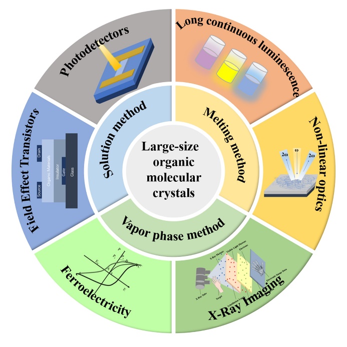
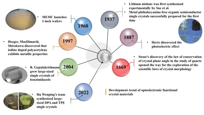
Organic molecular crystals, bounded together by non-covalent interactions, are three-dimensional long-range ordering and thermodynamic stable, and have low defect density and show rich prospects for applications in organic field effect transistors (OFETs), X-ray imaging, nonlinear optics, optical waveguides, flexible wearable devices, and lasers. However, previous research is mainly based on organic bulk crystals or small-size crystals, and there is less research on large-size organic molecular crystals while practical application scenarios often require large-size organic molecular crystals, such as transistor arrays and circuits requiring inch-level crystal films, X-ray imaging and nonlinear optical frequency conversion require centimeter-level crystals. However, it is difficult to obtain high-quality large-size organic molecular crystals, and there is no summary and review on the growth and optoelectronic properties of large-size organic molecular crystals at home and abroad. In this review, we first introduce the growth mechanism and growth method of molecular crystals, followed by the materials for growing large-size organic molecular crystals. Then we summarize the applications of large-size organic molecular crystals in optoelectronic aspects, such as long-persistent luminescence, nonlinear optics, X-ray imaging, fast neutron detection, field-effect transistors, and photodetectors. Finally, the challenges in this field are discussed and an outlook on future development is provided.
Contents
1 Introduction
2 Growth mechanism and method
2.1 Theory of crystal growth
2.2 Growth methods
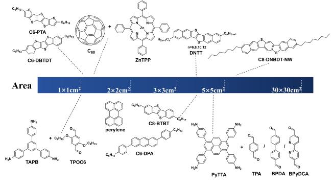
3 Classical organic molecular materials
3.1 Materials for Bulk single crystals
3.2 Materials for single crystal films
4 Optoelectronic applications
4.1 Long-Persistent Luminescence
4.2 Non-linear optical response
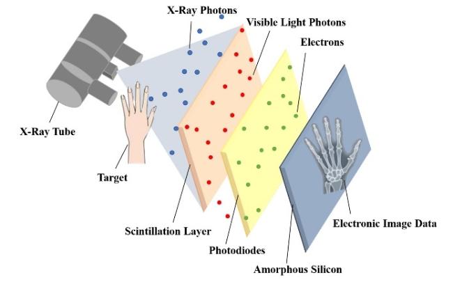
4.3 X-Ray Imaging
4.4 Fast neutron detection
4.5 Ferroelectricity
4.6 Field-Effect Transistors and Circuits
4.7 Photodetectors
5 Conclusion and outlook
Key words: molecular crystal; large size; optoelectronics; field effect transistor
Jingyu Cui , Hui Jiang , Rongjin Li , Weigang Zhu . Growth of Large-Size Organic Molecular Crystals for Optoelectronic Applications[J]. Progress in Chemistry, 2024 , 36(2) : 204 -223 . DOI: 10.7536/PC230616
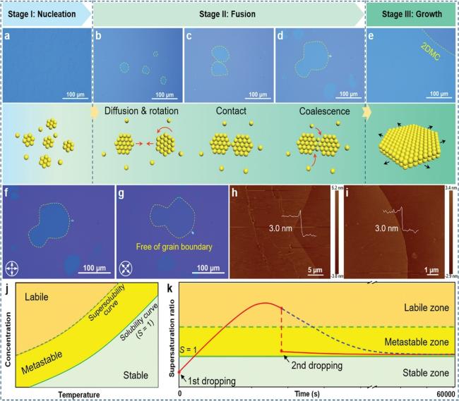
图2 非经典结晶在:a)成核,b~d)融合,e)生长阶段的光学显微镜图像。f, g)融合阶段凹形晶体的偏光显微镜图像。h, i)对应的AFM图像。j)典型浓度 - 温度曲线示意图。k)过饱和度作为时间的函数,通过两步法引入了S的阶跃变化[30]Fig.2 Optical microscope images of the nonclassical crystallization in the: a) nucleation, b~d) fusion, and e) growth stage. f, g) Polarizing microscope images of a concave-shaped crystal in the fusion stage. h, i) The corresponding AFM images. j) A schematic of a typical concentration-temperature curve. k) Supersaturation ratio as a function of time, by which a step-change of S was introduced by the two-step procedure[30]. Copyright © 2022 The Authors. Advanced Electronic Materials published by Wiley‐VCH GmbH |
表1 晶体生长技术总结Table 1 Summary of Crystal Growth Techniques |
| Crystal growth method | ||
|---|---|---|
| Melting method | Solution method | Vapor phase method |
| Bridgman method | High temperature solution growth | Physical vapor phase growth |
| Czochralski method | Low temperature solution growth | Chemical vapor growth |
| Stepanov method | Cosolvent method | Gas-liquid-solid method |
| Kyropoulos method | Hydrothermal method | Crystal growth by sputtering method |
| Flame fusion growth | Liquid phase electrodeposition method | Molecular beam epitaxial growth |
| MOCVD technology | ||
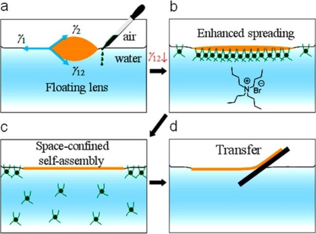
图5 二维分子晶体生长和转移的空间限制自组装法示意图。(a) 将液滴溶液置于去离子水表面形成漂浮透镜。(b) 在去离子水中使用表面活性剂增强扩散。(c) 二维结晶导致二维分子晶体的生长。(d) 二维分子晶体转移到目标基板[38]Fig. 5 Sketches of the SCS method for the growth and transfer of 2DMC. (a) A floating lens was formed when a droplet of solution was placed on the surface of DI water. (b) Enhanced spreading with surfactant in the DI water. (c) 2D crystallization resulted in the growth of 2DMC. (d) Transfer of the 2DMC to the target substrate[38]. Copyright © 2018, American Chemical Society |
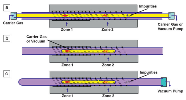
图7 物理气相传输生长方法 (a) 开放系统,材料在区域 1 中加热,并在几托(几百帕)到大气压的压力下在载气流中升华。分子蒸气在下游区域 2 中以较低的温度结晶,由于温度梯度和载气的流动,纯晶体与杂质分离。 (b) 封闭系统,材料(杂质和化合物)在密封的玻璃/石英安瓿中加热。 (c) 半封闭系统,这些材料密封在玻璃安瓿中,但安瓿中的小孔允许杂质和一部分结晶材料从安瓿中逸出。 1区:升华区; 2区:晶体生长区[48]Fig. 7 Scheme of the physical vapor transport growth method. (a) Open system. The material is heated in zone 1 and sublimed in a flow of carrier gas under pressures ranging from a few Torr (few hPa) to atmospheric pressure. The molecular vapor crystallizes downstream at a lower temperature in zone 2, with pure crystals separated from impurities due to the temperature gradient and the flow of the carrier gas. (b) Closed system. The material (impurities and the compound of interest) is heated in a sealed glass/quartz ampoule. (c) Semi-closed system. The materials are sealed in a glass ampoule, but a small orifice in the ampoule allows impurities and a portion of the crystallizing material to escape from the ampoule. Zone 1: Sublimation zone; zone 2: Crystal growth zone[48]. Copyright © 2013, The Materials Research Society |
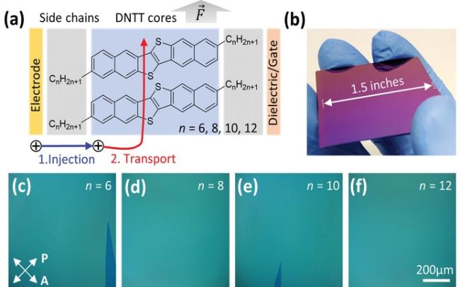
图12 a) 载流子在电极/Cn-DNTT 界面传输的示意图。b) 沉积在 SiO2 晶圆上的英寸大小的单层晶体。 c~f) n 分别为 6、8、10 和 12的Cn-DNTT 的单层晶体的 CPOM 图像。白色交叉箭头表示偏振器和分析器的位置[58]Fig. 12 a) Schematic process of carrier transport at the electrode/Cn-DNTT interface. b) Inch-sized 1L-crystals deposited on a SiO2 wafer. c~f) CPOM images of 1L-crystals of Cn-DNTTs, n = 6, 8,10, and 12, respectively. White crossed arrows denote the position of the polarizer and analyzer[58]. Copyright © 2022 Wiley‐VCH GmbH |
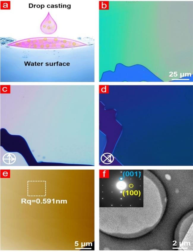
图13 a) 水滴浇铸水面示意图。b) ZCC共晶膜的光学显微镜图像。c)、d) ZCC共晶膜的偏光显微镜图像。e) 典型ZCC胶片的AFM图像。f) ZCC薄膜的TEM及其对应的SAED图像[64]Fig. 13 a) Diagram of drop-casting onto water surface. b) Optical microscope image of a ZCC cocrystal film. c), d) Polarized optical microscope images of the ZCC cocrystal film. e) AFM image of a typical ZCC film. f) TEM and its corresponding SAED images of a ZCC film[64]. Copyright © 2020 Wiley‐VCH GmbH |
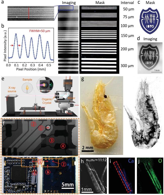
图16 有机半导体单晶在X射线成像中的实际应用。a) 由9,10-DPA晶体拍摄的线性掩膜的X射线图像。b) 像素的光强函数(沿上面的红线,FWHM作为分辨率)图案的毫米级掩模。 c, d) 基于9,10-DPA单晶的X射线探测器为大学标志拍摄的X射线图像。e)由X射线同步辐射源激发的系统示意图。f) 电路板的X射线成像;红色数字表示相应的位置照片和X射线成像。g) 小虾米干的X射线成像。h) 小虾干的SEM图像。i) 虾尾的钙元素图谱和j) 氧元素图谱[71]Fig. 16 Practical application of the organic semiconductor single crystals for X-ray imaging. a) X-ray images of linear mask taken by 9,10-DPA crystals. b) Light-intensity function of pixels (along the red line above and FWHM is taken as the resolution) patterned millimeter-scale mask. c, d) X-ray images taken by 9,10-DPA single-crystal-based X-ray detector for the university logo. e) System schematic excited by an X-ray synchrotron radiation source. f) X-ray imaging for the circuit board; the red numbers indicate the corresponding position photos and X-ray imaging. g) X-ray imaging for dried small shrimp. h) SEM image of dried small shrimp. i) Calcium mapping and j) oxygen mapping of the shrimp tail[71]. Copyright © 2021 Wiley‐VCH GmbH |
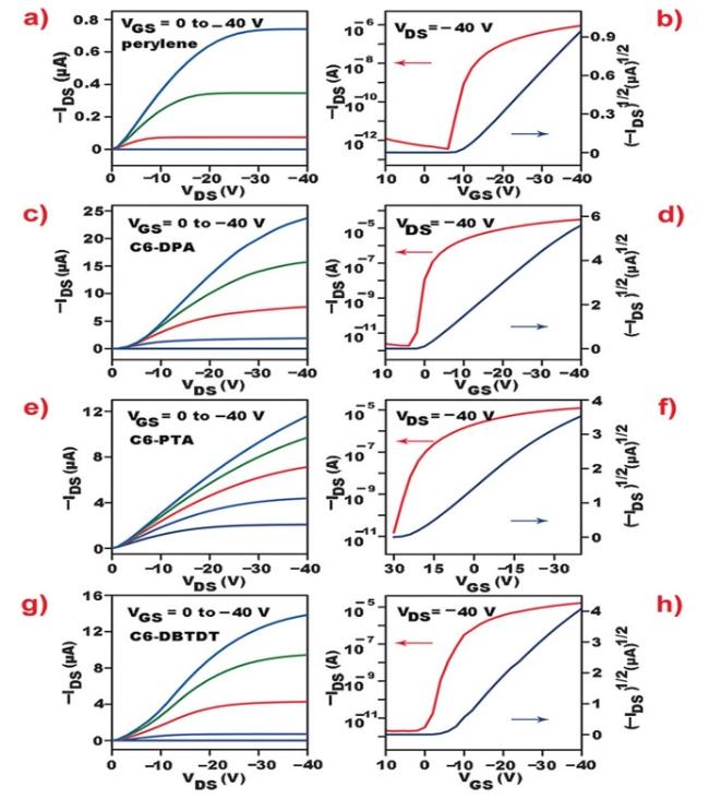
图18 2DCOS的晶体管特性。基于OTS SAM改性Si/SiO2衬底上的2DCOS,a)、b)苝,c)、d) C6-DPA,e)、f) C6-PTA,g),h) C6-DBTDT的OFET的典型传输和输出特性。(a)(c)(e)和(g)中的不同颜色的线对应于不同的栅极电压[81]Fig. 18 Transistor characteristics of the 2DCOS. Typical transfer and output characteristics of the OFETs based on the 2DCOS, a), b) perylene, c), d) C6-DPA, e), f) C6-PTA, g), h) C6-DBTDT on OTS SAM modified Si/SiO2 substrates. The different colored lines in (a) (c) (e), and (g) correspond to the different gate voltages[81]. Copyright © 2016 WILEY‐VCH Verlag GmbH & Co. KGaA, Weinheim |
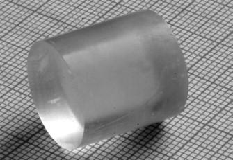
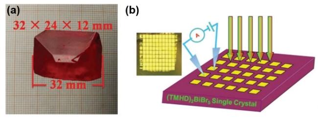
图19 (a) (TMHD)BiBr5的大块单晶照片。(b) 基于高取向(TMHD)BiBr5单晶的平面型单晶光电探测器器件示意图[83]。Fig. 19 (a) Photograph of a bulk single crystal of (TMHD)BiBr5. (b) Diagram of planar-type single-crystal photodetector device based on highly oriented (TMHD)BiBr5 single crystal[83]. Copyright © 2018 WILEY‐VCH Verlag GmbH & Co. KGaA, Weinheim |
| [1] |
|
| [2] |
|
| [3] |
|
| [4] |
|
| [5] |
|
| [6] |
|
| [7] |
|
| [8] |
|
| [9] |
|
| [10] |
|
| [11] |
|
| [12] |
|
| [13] |
|
| [14] |
(崔双月. 山东大学博士论文, 2021.)
|
| [15] |
(窦子凡. 电子科技大学硕士论文, 2022.)
|
| [16] |
|
| [17] |
|
| [18] |
|
| [19] |
|
| [20] |
汪卫华. 物理学进展, 2013, 33(5): 177.)
|
| [21] |
(赵九蓬. 新型功能材料设计与制备工艺. 北京: 化学工业出版社, 2003.)
|
| [22] |
(介万奇. 晶体生长原理与技术. 2版. 北京: 科学出版社, 2019.)
|
| [23] |
|
| [24] |
|
| [25] |
|
| [26] |
|
| [27] |
|
| [28] |
(郑燕青, 施尔畏, 李汶军, 王步国, 胡行方. 无机材料学报, 1999, 03: 321.)
|
| [29] |
施尔畏, 仲维卓, 华素坤, 元如林, 王步国, 夏长泰, 李汶军. 中国科学, 1998, 01: 37.)
|
| [30] |
|
| [31] |
|
| [32] |
|
| [33] |
|
| [34] |
|
| [35] |
|
| [36] |
|
| [37] |
|
| [38] |
|
| [39] |
|
| [40] |
|
| [41] |
|
| [42] |
|
| [43] |
|
| [44] |
|
| [45] |
|
| [46] |
|
| [47] |
|
| [48] |
|
| [49] |
|
| [50] |
|
| [51] |
|
| [52] |
|
| [53] |
|
| [54] |
|
| [55] |
|
| [56] |
|
| [57] |
|
| [58] |
|
| [59] |
|
| [60] |
|
| [61] |
|
| [62] |
|
| [63] |
|
| [64] |
|
| [65] |
|
| [66] |
|
| [67] |
|
| [68] |
|
| [69] |
|
| [70] |
|
| [71] |
|
| [72] |
|
| [73] |
|
| [74] |
|
| [75] |
|
| [76] |
|
| [77] |
|
| [78] |
|
| [79] |
|
| [80] |
|
| [81] |
|
| [82] |
|
| [83] |
|
| [84] |
|
| [85] |
|
| [86] |
|
| [87] |
|
| [88] |
|
/
| 〈 |
|
〉 |