Home Journals Progress in Chemistry
Progress in Chemistry

Abbreviation (ISO4): Prog Chem      Editor in chief: Jincai ZHAO

About  /  Aim & scope  /  Editorial board  /  Indexed  /  Contact  / 
Review

Experimental Preparation of Borophene and Its Application in Sensors

  • Shifan Chen ,
  • Yi Liu ,
  • Xiang Liu ,
  • Qian Tian ,
  • Guoan Tai , *
Expand
  • State Key Laboratory of Structural Mechanics and Control for Aerospace Structures, Laboratory of Intelligent Nano Materials and Devices of Ministry of Education, College of Aerospace Engineering, Nanjing University of Aeronautics and Astronautics, Nanjing 210016, China

Received date: 2024-01-26

  Revised date: 2024-04-02

  Online published: 2024-06-29

Supported by

National Natural Science Foundation of China(61774085)

Natural Science Foundation of Jiangsu Province(BK20201300)

Priority Academic Program Development of Jiangsu Higher Education Institutions.

Abstract

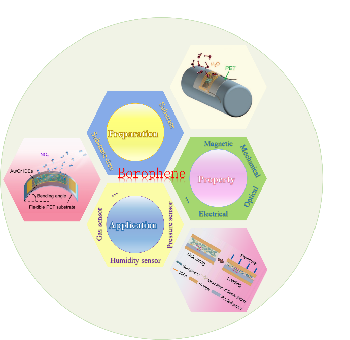
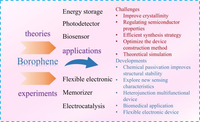
borophene,as an emerging single-element two-dimensional material,has attracted great interest from researchers due to its excellent properties such as high carrier mobility,mechanical compliance,optical transparency,ultrahigh thermal conductivity,and superconductivity.These properties make it an ideal candidate for research fields such as energy,sensors,and information storage.Guided by the pioneering experimental work in 2015,new achievements in experimental synthesis and practical applications of borophene continue emerging,which has driven the development of borophene from experimental synthesis to practical applications.based on the introduction of the special properties and innovative synthesis methods,we mainly review the application of borophene in the field of sensors.Finally,some reasonable discussions on potential issues and challenges for future researches are provided Based on the current state of research。

Contents

1 Introduction

2 Characteristics of borophene

2.1 Electrical properties

2.2 Optical properties

2.3 Mechanical properties

2.4 Magnetic properties

3 Preparation of borophene

3.1 Synthesis of borophene on substrate surface

3.2 Substrate-free synthesis of borophene

4 The application of borophene in sensors

4.1 Borophene gas sensor

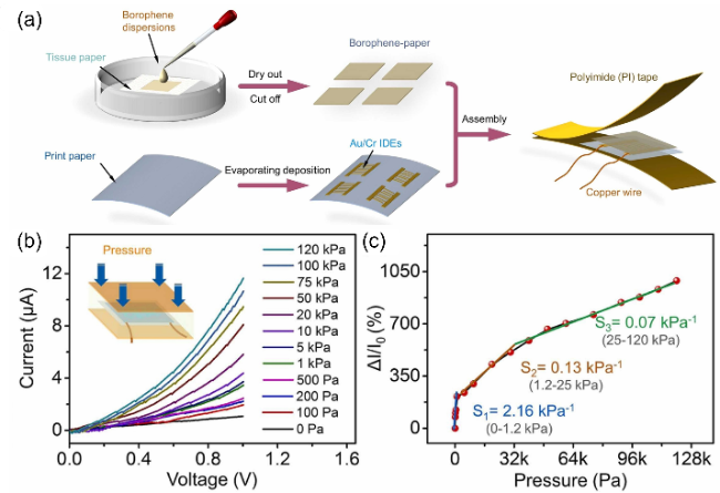
4.2 Borophene pressure sensor

4.3 Borophene heterojunction humidity sensor

5 Conclusion and outlook

Cite this article

Shifan Chen , Yi Liu , Xiang Liu , Qian Tian , Guoan Tai . Experimental Preparation of Borophene and Its Application in Sensors[J]. Progress in Chemistry, 2024 , 36(8) : 1119 -1133 . DOI: 10.7536/PC240122

1 Introduction

With many excellent properties,two-dimensional materials hold great potential for integration into next-generation electronic,sensing,and energy storage devices[1]。 Since the discovery of graphene,many two-dimensional materials have been successfully synthesized in the laboratory,such as silicene,germanene,phosphorene,hexagonal boron nitride and transition metal dihalides[2][3~5][6,7][8~10][11,12][13,14]。 Researchers have explored various kinds of two-dimensional materials in an endless stream,and Table 1 shows the characteristics and potential applications of various new two-dimensional materials[15~21]。 As neighbors of C in the periodic table,B and C share many similar features,including similar valence orbitals and the flexibility to adopt sp2hybridization to form low-dimensional structures.Therefore,the study of experimentally exploring the preparation of borophene has attracted great attention of researchers for a long time 。
表1 Characteristics and Applications of New Two-dimensional Materials[15~21]

Table 1 Characteristics and applications of two-dimensional materials[15~21]

2D Materials Structural characteristics Physical characteristics Potential application ref
Borophene Structural diversity
More stable after hydrogenation
Dirac cones
Larger Young’s modulus
Superconductivity
Energy storage
Nanoscale gas sensor
Biomedical applications
15
Silicene Low buckled geometry Dirac cones
High Fermi velocity and carrier mobility
Spin-orbit coupling
Ambipolar Dirac charge transport
Field effect transistor
Spintronic devices
16
Germanene Low buckled geometry Resistance to atmospheric oxidation Energy storage and catalysis 17
Phosphorene Vertically skewed/wrinkled honeycomb structure Semiconductor with a predicted direct bandgap
Layer dependent photoluminescence
Superior mechanical flexibility
Phosphorene-based devices 18,19
Hexagonal boron nitride Hexagonal structure Electrical insulation
Excellent thermal conductivity
Substrates and gate dielectrics for 2D electronics applications
Super-capacitor
20
Transition metal dihalides Containing triangular and honeycomb transition metal nets High temperature paramagnetic behavior Kitaev spin liquid 21
In fact,the theoretical study of borophene is much earlier than its experimental preparation,and the early study of borophene is mainly focused on various B atom clusters.Depending on the cluster size,B clusters can exhibit planar,quasi-planar,or cage-like structures.Smaller sized B clusters(n<15,n is the number of atoms)usually form planar or quasi-planar structures,such as B8-and B9-[22][23]。 While the larger B clusters(n≥28)adopt a similar symmetric cage configuration as C,for example,neutral B40with a fullerene-like cage has been shown to be more stable than its planar isomer[24]。 In contrast,the structure of B80buckyball is more spherical,and its structure is similar to that of C60buckyball[25]; While the larger B clusters(n≥80)have a shell structure of B12icosahedron[26~28]。 In addition,many studies have theoretically explored the possible formation of two-dimensional borophene structures.Boustani proposed that the structure with a bent triangular pattern is the most stable two-dimensional borophene structure[29]。 Subsequently,two research groups respectively proposed to obtain stabilizedα-boron nanosheets by unfolding the B80buckyball into a planar structure[30,31]。 On this basis,by using the first-principles particle swarm optimization(PSO)global algorithm,Wu et al.Predicted that the two boron monolayers(α1-andβ1-sheets)are the most stableαandβ-type boron nanosheets,respectively[32]。 This study also revealed the metallic properties ofα1-,β1-,g1/8-,and g2/15-B monolayers and the semiconducting properties ofαmonolayers.These properties have led researchers to turn their attention to experimental synthesis.In recent years,many researchers have successfully prepared two-dimensional borophene on various metal substrates,and have creatively developed new ways to prepare two-dimensional borophene,such as thermal decomposition and liquid phase exfoliation[33][34~47]。 in addition,there are endless studies on the excellent properties of borophene in electricity,optics,mechanics and magnetism.Based on these excellent characteristics,researchers have explored the broad application prospects of borophene in sensors,photodetectors,memristors and electrochemistry[34,48~52][34][34,53~55][15,34]
With the rapid development of modern microelectronics and nanotechnology,the innovation and upgrading of sensor technology has attracted wide attention from academia.borophene,as a new star in two-dimensional materials,has excellent properties in electricity,optics,magnetism and mechanics.in fact,many theoretical studies have predicted the outstanding performance of borophene in sensors,which also laid an important foundation for the application of two-dimensional borophene in the field of sensors[56,57]。 However,there are limited reports on the application of borophene and its heterostructures in the field of sensors.based on this,our group has done some important research on the application of borophene in various sensors.Therefore,this review mainly introduces the progress in the experimental preparation of borophene in recent years,and reveals its potential applications in the field of sensors Based on its excellent performance。

2 Properties of borophene

2.1 Electrical property

Borophene has unique physicochemical properties and diverse structures due to the prominent electronic defect characteristics of boron atoms and their tendency to form a variety of multicenter bonds.Based on the local density approximation theory,Penev et al.Predict that most two-dimensional borophene is metallic,and calculate the electron-phonon coupling strength of several two-dimensional borophene to estimate the superconducting critical temperature Tcof two-dimensional boropene,and the results show that two-dimensional boropene is a conventional superconductor[58]。 In addition,Feng et al.Successfully synthesizedβ12single layer boron film on Ag(111)surface,and confirmed the existence of metal boron-derived band by angle-resolved photoemission spectroscopy[59]。 The Fermi surface consists of an electron band at the$\bar{S}$point and a pair of hole bands near the$\bar{X}$point,which successfully confirms the metallic nature of 2D borophene.Inspired by graphene,people have extensively searched for new Dirac materials.Feng et al.Have studiedβ12-B thin films in detail in theory and experiment,and proved that the lattice ofβ12-B thin films can be decomposed into two triangular sublattices in a way similar to honeycomb lattice,thus carrying Dirac cones[60]。 This study further demonstrates that two-dimensional borophene has graphene-like metallic properties.However,the metallic nature of borophene severely limits its potential application In semiconductor information devices.in 2012,based on the Perdew-Burke-Ernzerhof(PBE)functional and the PBE 0 functional,Wu Xiaojun et al.of the University of Science and Technology of China discussed a slightly curvedα-B monolayer,calledααʹ-B monolayer[32]。 It is found that theααʹ-B monolayer not only has a higher cohesive energy than theα-B monolayer,but also is a semiconductor material with an indirect band gap,which lays a theoretical foundation for the device application of semiconductor borophene.in addition,our group has also studied the electrical properties of borophene In depth,and the results show that the synthesized borophene has semiconductivity[61]。 This provides an important support for the application of borophene in the field of electronic information devices。

2.2 Optical property

Borophene exhibits significant in-plane optical anisotropy due to its anisotropic atomic structure[62]。 In the visible region,the reflectivity of borophene is highly orientation-dependent.A strong energy and thickness dependent optical transparency was observed for the polymorphsβ12andδ6of borophene,both phases exhibiting low absorbance(<1%)in the visible range[63]。 Lherbier et al.compared the optical conductivity of borophene with that of graphene,and studied the optical properties of borophene in various wavelength ranges[64]。 The optical conductivity of borophene is close to zero for low energy radiation up to 3 eV,which is lower than that of monolayer graphene.However,the optical conductivity of borophene in the ultraviolet region increases slowly;The transmittance and reflectance of borophene in the infrared region are close to zero.The special properties of borophene in different optical regions make it promising for applications in optical devices。

2.3 Mechanical property

in fact,a large number of two-dimensional materials have been Used in flexible electronic devices,and the excellent mechanical properties are the basis for their wide application in the field of flexible electronics.Wang et al.used first-principles density functional theory to study the ideal tensile strength and critical strain of monolayer borophene in a and B directions[65]。 It is found that monolayer borophene can withstand stresses up to 20.26 and 12.98 N/m In the a and B directions,respectively.However,the critical strain is very small,only 8%in the a-direction,but the tensile strain applied in the b-direction increases the buckling height of borophene,resulting in a negative out-of-plane Poisson's ratio,which makes borophene show excellent mechanical flexibility along the b-direction.in addition,Le et al.Studied the mechanical properties of borophene with five different vacancy ratios(0.1~0.15)by molecular dynamics simulation with ReaxFF force field[66]。 It is found that the Young's modulus and tensile strength of borophene decrease with the increase of temperature.This study reveals the relationship between the mechanical properties of borophene and the loading direction,temperature,and atomic structure.Mortazavi et al.Analyzed the effect of loading direction and point vacancy on the mechanical properties of borophene[67]。 the results show that borophene with different configurations shows a wide range of mechanical properties,for example,a significant elastic modulus in the range of 163 to 382 GPa·nm and a high ultimate tensile strength of 13.5 to 22.8 GPa·nm.Zhang et al.'s Study on the recently synthesized hollow hexagon(HH)borophene also shows that the mechanical properties of borophene can be further adjusted by changing the concentration of HH[68]。 The high flexibility and elasticity of borophene provide unlimited possibilities for its application in various types of flexible sensing devices。

2.4 Magnetic property

For carbon,magnetic properties in highly oriented pyrolytic graphite with vacancies,graphite ribbon under electric field,and tetrakis(dimethylamino)ethylene fullerene have been reported.However,there are few reports on the magnetism of two-dimensional borophene,until 2016,Zhou et al.Theoretically calculated the two-dimensional antiferromagnetic boron(called M-boron),which is composed entirely of hexagonally arranged B20clusters[69]。 It is shown that the highest valence band of M-boron is isolated,strongly localized,and very flat,which induces spin polarization on either face of the B20cluster.This flat band originates from the unpaired electron of the capping atom,from which the magnetism arises.This study demonstrates that M-boron is thermodynamically metastable and is the first magnetic two-dimensional form of elemental boron.Otherwise,Jiang et al.Investigated the electronic structure and magnetic properties of 3D TM(TM=Ni,co,Mn,Fe,Cu,Zn,Sc,Ti,V and Cr)atoms adsorbed onβ12andχ3borophene by density functional theory(DFT)calculations[70]。 This study provides a new idea for the magnetic study of borophene。

3 Preparation of borophene

At present,a large number of theoretical simulation results on borophene strongly guide its various preparation strategies.Experimentally,the reported synthesis methods of borophene mainly include chemical vapor deposition(CVD),physical vapor deposition(PVD),in situ thermal decomposition,liquid phase exfoliation,and solvent/hydrothermal methods。

3.1 Synthesis of Borophene on Substrate Surface

borophene alone is metastable in nature,and a metal substrate with moderate binding strength with boron atoms is needed for the deposition of two-dimensional borophene.Although the possibility of growing borophene on various metal substrates has been theoretically confirmed for a long time,it is only in recent years that researchers have successfully prepared two-dimensional borophene on Ag(111),Ag(100),Ag(110),Cu(111)and other substrates[71~73][74][75][76,77]
In 2015,Tai et al.Successfully prepared borophene thin films using a self-made two-temperature zone chemical vapor deposition equipment(Figure 1 a)[61]。 In order to control the growth rate,the temperatures of the source region(T1)and the substrate region(T2)were separately controlled,and the mixture of B and B2O3powders was annealed to produce boron dioxide(B2O2)vapor.The copper foil is heated under T2=1000℃,so that the B2O2vapor carried by the H2is contacted with the surface of Cu which is close to a molten state,and the B2O2vapor is reduced into B atoms by the H2and deposited on the surface of the copper foil to adsorb,nucleate and grow a borophene film.The structure of the film consists of icosahedral B12units and B2dumbbells(Fig.1 a),and it has an orthorhombicγ-B28unit cell containing 28 atoms(a=5.054 054Å,B=5.620 620Å,C=6.987 987Å).The AFM image shows a typical borophene film thickness of∼0.80 nm(Figure 1 B).The fast Fourier transform(FFT)image shows the high crystallinity of the film and the characteristics of the orthorhombic structure(Fig.1 C),and the three FFT diffraction bright spots can be indexed to the(011),($\bar{011}$),and(020)crystal planes of the orthorhombicγ-B28structure,respectively,which is in good agreement with the structural parameters calculated by the first principle.In the UV-Vis absorption spectrum,a characteristic absorption peak at 614 nm is observed(Fig.1 d),and the room temperature photoluminescence(PL)spectrum shows a large,sharp emission band centered at 626 nm(Fig.1 e),with a corresponding optical band gap estimated to be 2.25 eV.These results show that the prepared two-dimensional borophene has semiconductor properties,and its application potential in the fields of photodetectors,LEDs,logic devices and sensors can not be underestimated 。
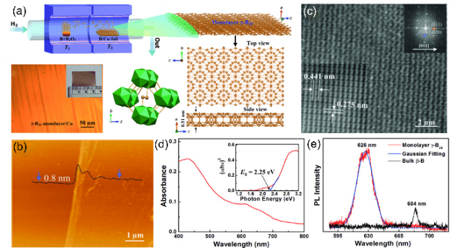
图1 γ-B28硼烯的示意图及物理特性表征:(a)γ-B28硼烯的制备与结构示意图;(b)AFM图像;(c)FFT图像;(d)紫外-可见(UV-Vis)吸收光谱;(e)室温光致发光(PL)光谱[61]

Fig. 1 Schematic diagram and physical characterization of γ-B28 borophene: (a) Schematic diagram of preparation and structure of γ-B28 borophene; (b) AFM images; (c) FFT images; (d) Ultraviolet-visible (UV-Vis) absorption spectrum; (e) Room temperature photoluminescence (PL) spectrum[61]. Copyright 2015 John Wiley and Sons

Almost at the same time,researchers found that Ag(111)can provide a good inert surface for the growth of borophene.Mannix et al.Have successfully grown two-dimensional borophene on Ag(111)substrate by molecular beam epitaxy(MBE)[71]。 the boron flux was kept between 0.01 and 0.1 monolayer per minute(ML)during the growth,and the substrate temperature was kept at 550°C(Fig.2a).the STM topography image(Figure 2 B)shows two different boron phases:a homogeneous phase and a corrugated"stripe phase".the dI/dV map given in Fig.2 C(where I and V are the tunneling current and voltage,respectively)shows a strong electronic contrast between borophene and Ag(111)substrate.More homogeneous phases can be observed at higher deposition rates(Fig.2 d,e),while increasing the growth temperature also favors the formation of stripe phases,with the substrate completely covered by borophene and boron clusters when the boron coverage is close to 1.0 ML(Fig.2 f,G)。
图2 Ag(111)衬底上生长硼烯:(a)制备硼烯的MBE装置示意图;(b)~(g)硼烯的STM图像(左)和闭环dI/dV图(右) [71]

Fig. 2 Synthesis of borophene on Ag (111) substrate: (a) Schematic diagram of MBE device for preparing borophene; (b) ~(g) STM image of borophene (left) and closed-loop dI/dV (right)[71]. Copyright 2015 Science

After that,the experimental studies on the synthesis of two-site borophene on various substrates have been reported successively.Wu et Al.Successfully prepared pure honeycomb lattice two-dimensional boron structure by molecular beam epitaxy using Al(111)surface as substrate[78]。 A monolayer of borophene is formed by evaporation of boron atoms onto an al(111)substrate at a temperature of about 500 K.High-resolution scanning tunneling microscopy images show that the surface of the boron monolayer has a typical periodic triangular corrugation,and the measured lattice constant is 0.29 nm.the honeycomb lattice is locally flat,and the atomic corrugation(~1.5 pm)In the honeycomb lattice overlapped on the periodic triangular corrugation is much smaller than the triangular corrugation(40~60 pm),which indicates that the honeycomb borophene monolayer is obtained on the Al(111)substrate.in 2019,Vinogradov et Al.successfully grew a two-dimensional boron structure on the Ir(111)surface[79]。 This borophene structure is ofχtype with HH densityη=1/6.The borophene unit cell has an area of 76.408Å2and a density of 0.327Å-2,which also fits well with otherχ-type structures 。
In addition to the growth of Borophene on metal substrates such as Cu(111),Ag(111),Al(111)and Ir(111)introduced above,our group has also creatively attempted the growth of borophene on functional substrates.borophene was successfully grown on mica substrate by chemical vapor deposition and applied to photodetectors[80]。 In a typical growth process,the annealed sodium borohydride(NaBH4)precursor powder is partially volatilized and decomposed into B atom clusters,which are subsequently transported to the deposition zone by H2and diffused to the mica surface to reassemble into borophene structure.The corresponding structure of the synthesizedα′-2H borophene is shown in Fig.3 B.Figure 3 a shows the atomic configuration of borophene and the possible arrangement of borophene on mica.The(001)planes of the B capping layer and the mica substrate have high in-plane symmetry,and the lattice mismatch between the B capping layer and the mica substrate is less than 5%,which indicates that borophene and mica have similar lattice structures,which will induce the epitaxial growth of borophene on mica.The AFM results show that borophene is highly homogeneous,with a thickness of∼1.7 nm(Figure 3C).The TEM characterization revealed the structure of borophene,and the HRTEM image showed that borophene was a uniform film,and the corresponding FFT pattern showed that the interplanar spacing of borophene was about 4.34 and 4.3838Å(Figure 3D).In addition,Figure 3 e shows the HRTEM image of the thicker region of borophene,and the inset in the upper right corner is the corresponding selected area electron diffraction(SAED)pattern.The results can be indexed to the(100),(110),and(010)crystal planes ofα′-2H borophene,respectively.The corresponding lattice matches the theoretical DFT-based first-principles calculation results perfectly 。
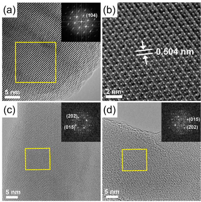
图3 云母衬底上硼烯的晶体结构:(a)硼烯和云母的原子结构图;(b)α′-2H硼烯的结构;(c)硼烯的AFM图像;(d)硼烯的HRTEM图像;(e)硼烯的TEM图像。插图为相应的SAED图像[80]

Fig. 3 Crystal structure of borophene on mica substrates: (a) Atomic structure diagram of borophene and mica; (b) Structure of α′-2H borophene; (c) AFM image of borophene; (d) HRTEM image of borophene; (e) TEM image of borophene. Corresponding SAED images are shown as insets[80]. Copyright 2021 ACS Publications

Molecular beam epitaxy(MBE)and Chemical vapor deposition(CVD)are the common methods for the preparation of borophene on substrates.Molecular beam epitaxy(MBE)generally uses pure boron source as the raw material for the synthesis of borophene,which has high crystallinity and thin thickness,but requires strict experimental conditions,low synthesis efficiency and high cost.chemical vapor deposition can synthesize borophene with high efficiency and lower cost,but the quality of the synthesized borophene is difficult to control.During the synthesis of borophene by these two methods,the lattice matching and charge transfer between borophene and substrate will affect the structure and morphology of borophene.in addition,the borophene synthesized on the substrate is difficult to be stripped from the substrate,and in general,it is easy to be oxidized in the air。

3.2 Substrate-free synthesis of borophene

Because expensive substrates are usually used in the process of growing borophene on substrates,and the samples are damaged to varying degrees during the transfer process,researchers have Developed new low-cost synthesis strategies to obtain two-dimensional borophene,such as liquid phase exfoliation and thermal decomposition.Li et al.developed a scalable liquid-phase exfoliation technique for producing high-quality few-layer boron nanosheets[81]。 the experimental process can be summarized as follows:firstly,bulk boron powder with an average lateral particle size of 2μm was immersed in DMF or IPA solvent and tip sonicated for 4 H at a power of 350 W;Then,in order to adjust the concentration and thickness of the boron nanosheets,the sonicated boron nanosheets were centrifuged at different centrifugal speeds,and the treated supernatant was collected.after centrifugation at 5000 R/min for 30 min,a stable light brown dispersion suspension could be obtained in both DMF and IPA solvents.Fig.4 a is a HRTEM image of a representative single B nanosheet After exfoliation in DMF solvent.the high crystallinity of the few-layer B nanosheets is further evidenced by the FFT pattern of Figure 4 B,showing that the interplanar spacing of the boron nanosheets is 0.504 nm,and these features correspond to the(104)plane of theβrhombohedral boron structure.Fig.4 C,d shows the HRTEM images of B nanosheets exfoliated utilizing IPA solvent.the lattice spacings of the two B nanosheets exfoliated by IPA are 0.427 and 0.435 nm,corresponding to the(015)and(202)planes of theβrhombohedral boron crystal,respectively.This study shows that few-layer boron nanosheets can be successfully exfoliated from bulk boron by ultrasound-assisted liquid phase exfoliation。
图4 在DMF(a, b)和IPA(c, d)中进行尖端超声处理4 h后,分别在5000 r/min下离心30 min,所制备的少层B纳米片的典型TEM图像。(a)、(c)和(d)的插图显示了所选区域相应的FFT模式[81]

Fig. 4 Typical TEM images of few-layer B nanosheets prepared by 4 h tip ultrasonication in DMF (a, b) and IPA (c, d), followed by centrifugation at 5000 r/min for 30 min. The insets in (a), (c), and (d) display the corresponding FFT patterns of the selected regions[81].Copyright 2018 ACS Publications

Based on the liquid phase exfoliation method,our group found that the fluffy high-purity boron powder can not only form nanosheets in IPA and DMF solvents,but also obtain borophene quantum dots in acetonitrile[43,82]。 As a pioneer work in the field of zero-dimensional borophene quantum dots,It has been promoting the development of low-dimensional boron in recent years.it can be seen that the liquid phase exfoliation method seems to be a simple and effective method for the preparation of boron nanosheets in large quantities,but related studies also show that the prepared boron nanosheets are not only difficult to accurately control the thickness and lateral size,but also have a large deviation from the current mainstream borophene structure。
Focusing on the new challenge of large-scale preparation of high-quality two-dimensional borophene,our group creatively used the method of in-situ thermal decomposition to successfully prepare two-dimensional borophene:Hou et al.Developed a three-step heating process to synthesize a large amount of hydrogenated borophene by in-situ thermal decomposition NaBH4[83]
A large amount of borylene hydride was synthesized by thermal decomposition of NaBH4powder step by step.In the first step,the powder was heated from room temperature to 490℃at a rate of 10℃/min for 2 H to form the initial state;The second step is to continue heating to 550℃at a rate of 5℃/min and keep the temperature for 30 min to form a more stable intermediate;In the third step,the intermediate was heated to 600℃at a rate of 5℃/min and kept for 30 min to produce a large amount of borophene.High-magnification scanning electron microscopy(SEM)images(Figure 5A)show that the thickness of borophene can be reduced to less than 1 nm by this new process.The statistical results show that the average lateral size of the flake is around 5.14µm(Fig.5 B).AFM characterization results show that the thickness of a typical flake is close to 0.78 nm,and the thickness distribution is between 0.78 and 3.50 nm,with an average thickness of about 1.8 nm(Figure 5C).A typical TEM image shows that the transverse dimension of this flake is more than 10μm(Figure 5D).The HRTEM image and the corresponding SAED mode confirm that this borophene is a single crystal.The HRTEM image extracted from the red rectangular region in Figure 5 e was reconstructed by masking the two-dimensional FFT mode,and the reconstructed image showed borophene structures with lattice spacings of about 4.31 and 4.3636Å(Figure 5 f).In addition,the results of first-principles calculations based on DFT show that the vacancy concentration of 1/9 ofααʹ-borophene is bonded to four hydrogen atoms,and the structure only exhibits a buckled configuration,which matches the experimental results.Compared with the on-substrate preparation method,borophene with stable structure in air can be obtained by chemical passivation,and borophene films can be prepared at low cost by either liquid phase exfoliation or thermal decomposition,but the crystallinity of the sample in large area needs to be improved.For micro-and nano-scale devices with low crystallinity requirements,borophene prepared in large quantities by these methods can better meet the test requirements,but the preparation of large area and high-quality borophene crystals needs a lot of exploration work 。
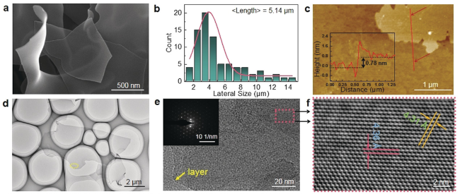
图5 原位热分解合成αʹ-4H-硼烯:(a)SEM图像;(b)扫描电镜测得的80张纳米片横向尺寸统计数据;(c)AFM图像;(d)低分辨率TEM图像;(e)HRTEM图像和相应的SAED图像;(f)对(e)中红色矩形区域提取的FFT模式进行重构后的HRTEM图像[83]

Fig. 5 Synthesis of αʹ-4H-borophene by in-situ thermal decomposition: (a) SEM image; (b) Statistical data of lateral dimensions of 80 nanosheets measured by SEM; (c) AFM image; (d) Low-resolution TEM image; (e) HRTEM image and corresponding SAED pattern; (f) Reconstructed HRTEM image of the FFT pattern extracted from the red rectangular region in (e)[83]. Copyright 2020 John Wiley and Sons

Otherwise,Shao et al.Successfully prepared borophene functionalized Fe3O4core-shell nanostructures by heating a mixture of Fe3O4nanoparticles and NaBH4powder on the basis of pretreated homogeneous Fe3O4nanoparticles[84]。 NaBH4powders volatilize continuously and controllably at high temperature and grow epitaxially on the surface of Fe3O4,which is an ideal way to coat Fe3O4nanoparticles.Room temperature photoluminescence(PL)spectra show that borophene functionalized Fe3O4core-shell nanoparticles are excellent semiconductor materials,based on which researchers have developed non-volatile memory with excellent performance 。
the integration of different two-dimensional materials is essential for nanoelectronics applications.in contrast to vertical stacking,covalent lateral splicing requires bottom-up synthesis,which leads to experimental difficulties In realizing two-dimensional lateral heterostructures.However,borophene is expected to be an ideal candidate for The synthesis of two-dimensional heterostructures due to its structural polymorphism and abundant bonding modes。
in the field of borophene heterojunction,our group has also done a lot of pioneering work,and successfully grown a large-scale borophene-graphene heterostructure In hydrogen environment[85]。 The NaBH4powder and the graphene are mixed according to a mass ratio of 100:1 and then are subjected to in-situ thermal decomposition in chemical vapor deposition equipment,and the borene-graphene heterostructure without any metal substrate is prepared under controllable conditions.The morphologies of graphene,ααʹ-4H-borophene,and borophene–graphene heterostructures were characterized by SEM(Fig.6 a–C).Unlike graphene or borophene,the borophene–graphene heterostructure exhibits an inhomogeneous hierarchical structure,and a large number of ultrathin borophene nanosheets can be observed on the outer surface of multilayer graphene,indicating the growth of borophenes on the graphene surface(Figure 6 C).A typical TEM image shows that borophene is in close contact with the layered graphene film without obvious agglomeration,indicating the coexistence of borophene and layered graphene(Figure 6 d).The HRTEM image and the corresponding SAED map show that the SAED spots are mainly from borophene(Fig.6 e,f).Figure 6G~I shows the HAADF-STEM element mapping at different positions of the vertical heterostructure.The HAADF image shows a typical stacked flake composed of borophene and graphene,with B and C atoms distributed in the corresponding regions,which further confirms the growth of borophene on the surface of few-layer graphene 。
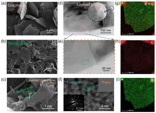
图6 硼烯-石墨烯异质结构的形貌和结晶度:(a~c)少层石墨烯、硼烯和硼烯-石墨烯异质结构的SEM图像;(d)典型异质结构的低分辨率TEM图像;(e)硼烯的低分辨率TEM图像;(f)从(e)中绿色矩形区域提取的HRTEM图像。插图为从计算模型中提取的相应SAED图像和HRTEM图;(g~i)异质结构的STEM-HAADF-EDS元素映射[85]

Fig. 6 Morphology and crystallinity of borophene-graphene heterostructures: (a~c) SEM images of few-layer graphene, borophene, and borophene-graphene heterostructure; (d) Low-resolution TEM image of a typical borophene-graphene heterostructure; (e) Low-resolution TEM image of borophene; (f) HRTEM image extracted from the green rectangular region in (e). Insets show the corresponding SAED patterns and HRTEM images obtained from computational models; (g~i) STEM-HAADF-EDS elemental mapping of the borophene-graphene heterostructure[85]. Copyright 2020 Springer Nature

4 Application of borophene in sensor field

4.1 Borophene gas sensor

Two-dimensional materials are excellent candidates for gas sensing due to their large specific surface area and the ability of charge transfer between gas and surface.To investigate the adsorption behavior of gases such as CO,CO2,NO,NO2,and NH3on borophene,Shukla et al.Tried the adsorbability of each gas molecule with respect to all configurations of borophene[86]。 Among the studied gases,the adsorption of CO2on the borophene surface is the weakest,and its bonding is considered to be weak physisorption;On the contrary,the adsorption energy of NO2is the largest;However,the binding energies of CO,NO and NH3are in between,and they are relatively strong chemisorptions with borophene.The charge density plots in Figure 7 a~e illustrate that the gas(except CO2)has a strong bonding effect on the borophene surface.In addition,the charge transfer between gas and borophene(Bader charge)shows that among all the gases,only the charge transfer of CO2gas is negligible,while a considerable amount of charge transfer between other gas molecules and borophene substrate can be observed,which further indicates the sensitivity of borophene to gas detection.Adsorption of gas molecules leads to a decrease in transmittance(Figure 7 f),attributed to backscattering suppressing the available conduction channels.CO and CO2have little effect on the transmission function,while NO,NO2and NH3have great effect on the transmission function of pristine borophene.From the point of view of designing sensors,borophene may be more sensitive to gases containing N elements such as NO,NO2,and NH3.In addition,a boron-based sensor device for gas detection based on current-voltage(I-V)characteristics was designed from a theoretical point of view.Fig.7G shows the I-V characteristics of all gas-borophene structures below 1 V.The adsorption resistance of gas molecules(CO,NO,NO2and NH3))increases,which is reflected by the decline of the current signal.The presence and absence of the gas is manifested in the form of significant current changes,specifically,the presence and absence of the gas can be considered as the on and off States of the device,which provides a theoretical basis for the performance evaluation of high-sensitivity borophene sensing devices 。
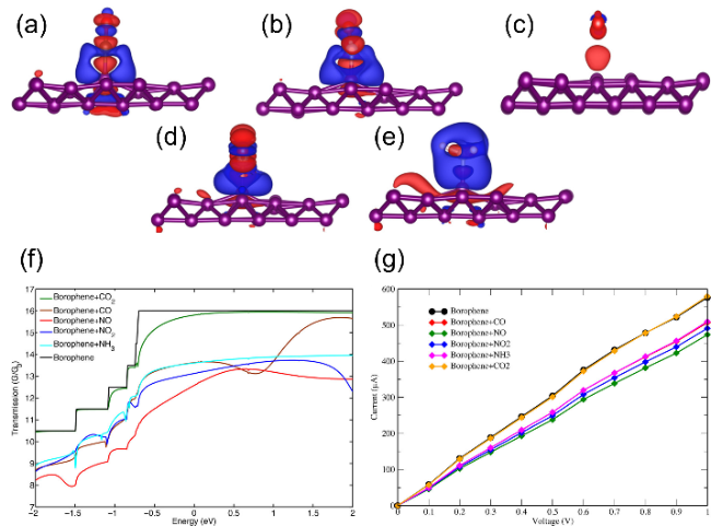
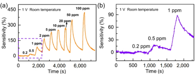
图7 (a~e)硼烯表面气体吸附(CO、NO、CO2、NO2、NH3)的电荷密度差图。红色表面表示电子获得,蓝色表面表示电子损失;(f)零偏压传输原始硼烯和硼烯+气体系统;(g)硼烯单层随不同吸附气体分子变化的I-V特性曲线[86]

Fig. 7 (a~e) Charge density difference maps of gas adsorption (CO, NO, CO2, NO2, NH3) on the surface of borophene. Red surfaces indicate electron gain, while blue surfaces indicate electron loss; (f) Zero-bias transmission of pristine borophene and borophene+gas system; (g) I-V characteristics of monolayer borophene with different adsorbed gas molecules[86].Copyright 2017 ACS Publications

Hou et al.Developed a NO2gas sensor based on borophene,based on the reasonable prediction that borophene has high sensitivity to gases containing N elements in theory[92]。 The real-time response of the borophene sensor at different NO2concentrations in dry air at room temperature is shown in Figure 8 a,and the concentration of NO2varies from 0.2 to 100 ppm.As the concentration of NO2increases,the sensitivity of the sensor gradually increases,especially in the concentration range of 0.2–1 ppm(Fig.8B).The sensitivity of the borophene gas sensor is basically unchanged under the cycle test of 50 ppm and 2 ppm NO2gas at room temperature,which indicates that the borophene gas sensor has good stability in the atmospheric environment at room temperature.NO2gas is a typical oxidizing gas,while borophene is a p-type semiconductor.When the NO2gas is injected,the adsorbed NO2molecules can generate more holes on the conduction band of borophene,thus increasing the conductance of borophene,which is mainly attributed to two factors:Schottky barrier and charge transfer.In addition,the adsorption and desorption of NO2molecules on the borophene surface is responsible for the charge transfer,which leads to a shift of the Fermi level toward the valence band of borophene 。
图8 硼烯气体传感器:(a)不同NO2浓度下的响应;(b)低NO2浓度时的响应[92]

Fig. 8 Borophene gas sensor: (a) Response curve at different NO2 concentrations; (b) Response curve at low NO2 concentration[92]. Copyright 2021 Springer Nature

In addition,some typical two-dimensional materials are also used in the field of gas sensing.Table 2 shows the important performance parameters of these gas sensing material devices.It is found that the borophene NO2gas sensor has the highest sensitivity and lower detection limit,indicating the strong application potential of borophene in two-dimensional material gas sensor devices 。
表2 Performance comparison of typical two-dimensional material gas sensors[87~92]

Table 2 gas sensing performances of some typical two-dimensional Gas sensing materials[87~92]

Material Sensitivity Response/recovery Detection limit ref
Graphene 146% 255/975 s 1.2 ppm 87
rGO 250% 100/>3000 s 50 ppm 88
Phosphorene 290% 480/720 s 0.02 ppb 89
MoS2 182.5% 3500/3500 s 100 ppm 90
ZnO 11.2% 25/36 s 5 ppm 91
Borophene 422% 30/200 s 0.2 ppm 92

4.2 Borophene pressure transducer

the ability of the skin to sense and detect pressure is essential for an organism to establish an interaction with the external environment that can effectively distinguish between the shape of an object and the nature of its surface.Therefore,wearable,skin-like or skin-fittable pressure sensors are attracting researchers in related fields。
Hou et al.Successfully constructed a high-performance pressure sensor using a new two-dimensional semiconductor borophene as an active material[93]。 the flexible sensor can be fabricated by impregnating The prepared hydrogenated borylene dispersion into a paper towel with a porous structure,recyclability,and low cost。
A typical stack structure of the sensor device is shown in Figure 9 a.Figure 9 B shows the current-voltage(I-V)curves of the borophene pressure sensor at different static mechanical pressures.This output characteristic with a nonlinear curve is because of the formation of a Schottky barrier between the boron film and the gold/chromium electrode.When the static pressure increases from 0 kPa to 120 kPa,the slope of the I-V curve increases significantly,which means that the Schottky barrier height decreases.While for the dynamic pressure(Fig.9 C),the sensitivity of this sensor can reach 2.16 kPa-1when the loading pressure is lower than 1.2 kPa.The sensitivity decreases to about 0.13 kPa-1in the pressure range of 1.2–25 kPa;Due to the effect of block matrix deformation under higher pressure,the sensitivity decreases to about 0.07 kPa-1when the loading pressure is greater than 25 kPa.In addition,the sensor has a response time of 90 ms and a recovery time of 115 ms,which is beneficial to its application in real-time exercise monitoring and human-computer interaction interface.Moreover,the sensor also shows long-term stability and good repeatability in 1000 dynamic cycles.The results show that the sensor has the characteristics of high sensitivity(2.16 kPa-1),wide detection range(0~120 kPa),low detection limit(down to 10 Pa),low power consumption(about 0.6μW)and high repeatability(more than 1000 times).The sensor can also be used as a wearable electronic skin for health monitoring,speech recognition,and wireless detection of human motion 。
图9 硼烯压力传感器:(a)硼烯压力传感器的制造流程图;(b)静态压力下器件的响应;(c)传感器的灵敏度[93]

Fig. 9 Borophene pressure sensor: (a) Process flowchart for manufacturing the borophene pressure sensor; (b) Response characteristics of the sensor under static pressure; (c) Sensitivity of the sensor[93]. Copyright 2022 Elsevier

Recently,based on topological ideas,Zhou et al.Of Anhui University used patterned borene-bismurene derivatives as sensing layers to construct high-performance pressure sensors on flexible indium-doped tin oxide(ITO)substrates[94]。 It is found that the specific capacitance of the electrode increases by 2.483 times with the addition of borophene.The flexible pressure sensor thus constructed has a wide detection range(0~220 kPa),low response and recovery times(80 ms and 80 ms),and a high sensitivity(1.60 kPa-1)in a small pressure range of about 50~150 Pa.In addition,the capacitance of the device remains at 97.92%of the original value after 10 000 loading-unloading cycles.Subsequently,borophene-based wearable pressure sensors were used to monitor small changes in human motion in real time.When the finger is pressed continuously on the sensor surface,a clear capacitance response curve is produced.In addition,they also monitored common human movements such as frowning,swallowing and grasping,and the results showed that the wearable device could accurately and quickly identify pressure.The stable dynamic response results show that the borophene wearable pressure sensor has potential applications in the field of human motion and medical health monitoring 。

4.3 Borophene heterostructure humidity sensor

In order to enhance the stability of two-dimensional borophene and overcome the short circuit problem,researchers often choose MoS2semiconductors with 2 H phase as substrates to broaden their applications.The borophene-MoS2heterostructure has been designed theoretically and its stability has been verified[95]。 However,there are few reports on the application of borophene heterostructure sensors.Our group has done some innovative work:the first successful preparation of borophene-MoS2heterostructure and its application in the field of humidity sensors[96]。 As a new type of sensor,humidity sensor has been proved to be effective in real-time respiratory monitoring and respiratory diagnosis。
In addition to the borophene-MoS2heterostructure mentioned above,another humidity sensor was developed,and a borophene-graphene humidity sensor was fabricated using the prepared borophene-graphene heterostructure(Figure 10a )[96]。 the tests were conducted under different environments of 0%,11%,33%,43%,67%,75%and 85%relative humidity(RH)(Fig.10B).when the relative humidity increases in a wide range from 0 to 85%,the sensitivity of the sensor increases gradually,and the linear regression curve fitted to the experimental data reflects the relationship between the sensitivity and the humidity concentration(Fig.10 C).It can be seen that the sensitivity of the heterostructure sensor is more than 4200%when the experiment is carried out at 0~85%RH.However,this heterostructure sensor does not work when RH≥97%。
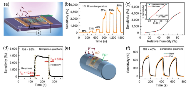
图10 硼烯-石墨烯异质结构湿度传感器:(a)基于硼烯-石墨烯异质结的传感器示意图;(b)不同相对湿度下异质结构传感器的湿度传感行为;(c)暴露于不同相对湿度下的异质结构传感器的灵敏度;(d)异质结构传感器在85% RH下的响应和恢复曲线;(e)PET衬底上弯曲异质结构传感器的示意图;(f)无弯曲应变和有弯曲应变时传感器的响应曲线[85]

Fig. 10 Borophene-graphene heterostructure humidity sensor: (a) Schematic representation of the sensor based on borophene-graphene heterostructure; (b) Humidity sensing behavior of the heterostructure sensor at different relative humidities; (c) Sensitivity of the heterostructure sensor exposed to different relative humidities; (d) Response and recovery curves of the heterostructure sensor under 85% RH; (e) Schematic diagram of the bent heterostructure sensor on a PET substrate; (f) Response curves of the sensor with and without applied bending strain[85]. Copyright 2020 Springer Nature

at 85%relative humidity,the sensitivity of the borophene–graphene sensor is about 27 times higher than that of the pristine borophene sensor,while the sensitivity of the borophene–graphene sensor is more than 699 times higher than that of the pristine graphene sensor.the time-dependent response and recovery curves of the borophene-graphene humidity sensor were tested at a relative humidity of 85%(Fig.10d)to obtain the response and recovery times,revealing the detection speed of water vapor:at 85%RH,the response and recovery times of the sensor were 10.5 s and 8.3 s,respectively.in addition,the sensing performance of the device under high bending strain was studied by replacing the rigid substrate with a flexible polyethylene terephthalate(PET)film(Figure 10 e),which was glued to the surface of a round bar(bending radius of 1 cm).Fig.10(f)shows that the borophene–graphene sensor at 43%RH shows a response of about 700%without bending strain.When the sensor is bent,the sensor can still work with a high response of about 710%.the above results demonstrate that the high flexibility of borophene-graphene makes it suitable for various application fields,especially In healthcare and wearable devices。
After that,Liu et al.Successfully fabricated borophene-BC2N heterostructure by ultrasonic self-assembly,and fabricated a high-performance humidity sensor by a facile and effective method[97]。 Figure 11A shows the real-time output current of the sensor during humidity switching.When the relative humidity increases from 0%to 97%,the current of the sensor increases significantly from 5.5 nA to 1.21μA,and the sensor shows ultra-high sensitivity(up to 22,001%at 97%RH)and a wide detection range(11%~97%).the results show that the sensitivity of the sensor can be accurately matched with any corresponding relative humidity,which is helpful to achieve accurate measurement of relative humidity。
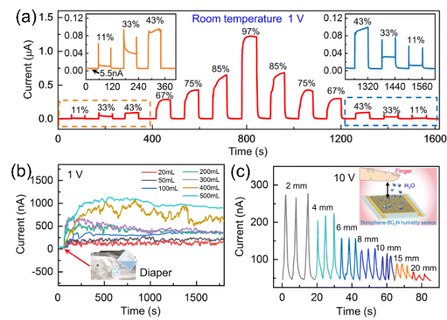
图11 硼烯-BC2N异质结构湿度传感器:(a)不同相对湿度下传感器的实时响应;(b)不同相对湿度下的长效响应;(c)指尖接近不同距离时传感器的实时电流曲线[97]

Fig. 11 Borophene-BC2N heterostructure humidity sensor: (a) Real-time response of the sensor at different humidity levels; (b) Long-term response of the sensor at different humidity levels; (c) Real-time current curve of the sensor as the fingertip approaches at different distances[97]. Copyright 2023 RSC Society of Chemistry

Based on the excellent humidity sensing performance of the sensor,it can be used in the fields of diaper monitoring for infants and critically ill patients,wireless monitoring of respiratory behavior,voice recognition and non-contact switch.As shown in Figure 11 B,20,50,100,200,300,400,and 500 mL of water were poured onto the diaper to simulate infant or patient enuresis.It is observed that the sensor can immediately respond to the rise of humidity,and the current will increase with the increase of water content,and maintain a high level of sensing response,which indicates that the sensor can accurately monitor the urine content in diapers,bringing convenience to the care of infants and bedridden patients.In addition,they attempted to apply the borophene-BC2N heterostructure to non-contact sensing.The relative humidity generated by the finger surface at different heights was detected from the sensor(Figure 11c),and it was observed that the sensor humidity response decreased as the finger moved away from the sensor.This work provides effective strategies for the development of smart diapers,auxiliary voice systems,human health monitoring and prevention,and promotes the development of non-contact human-machine interface systems without infection risk.In addition,Table 3 shows the sensing performance of previous two-dimensional material humidity sensors,which shows that the construction of borophene heterojunction is helpful to improve the humidity sensing sensitivity of borophene 。
表3 Performance Comparison of Typical Two-dimensional Material Resistive Humidity Sensors[85,97~101]

Table 3 humidity sensing performances of some typical two-dimensional material resistive Humidity sensors[85,97~101]

Material Sensitivity (%) Response (s) / Recovery (s) RH range
(%)
ref
Graphene 0.3 0.6/0.4 1~96 98
rGO 20.4 180/Irreversible 10~100 99
Black phosphorus 521 101/26 11~97 100
MoS2 2327 140/80 17.2~89.5 101
α'-4H-Borophene 150 2.3/0.7 67~85 85
Borophene-graphene 4200 10.5/8.3 0~85 85
Borophene-BC2N 22 001 11.82/1.41 11~97 97

5 Conclusion and prospect

in this paper,the development,excellent properties and preparation methods of two-dimensional borophene are reviewed,and the potential applications of two-dimensional borophene nanomaterials in the field of sensors are emphatically discussed.the growth of borophene on various substrates is presented,and it is found that the kind of borophene polymorph formed depends largely on the substrate choice,growth temperature,boron flux,and boron atom coverage.Experimentally,some progress has been made in the synthesis of borophene by CVD and MBE,but there is still much to be done in the preparation of structurally stable semiconductor borophene.in this regard,the study of stable and semiconductingααʹ-4H-borophene prepared by in-situ thermal decomposition method not only points out the direction for the preparation ofααʹ-phase borophene in large quantities,but also paves the way for the preparation method to improve the stability of borophene.in addition to pristine and functionalized borophene,borophene based heterostructures have received increasing academic attention.the theoretical prediction results show that borophene will be more stable when it forms heterostructures with other two-dimensional materials.Vertical and lateral heterostructures of borophene and graphene have great potential in the field of electronic device fabrication and integrated nanocircuits。
in addition to presenting reports on the experimental preparation of borophenes,This review also presents their physicochemical characteristics,aiming to tap into potential device applications.A large number of borophene allotropes have shown excellent properties,based on which researchers have explored their potential applications in the field of sensors,and found thatααʹ-4H-borophene and its heterostructures have excellent humidity-sensing,gas-sensing and pressure-sensing properties.Although some progress has been made in the research of borophene,the unique properties brought by the diversified structure of borophene need to be further explored.Therefore,we hope that the review of the application of borophene in the field of sensors in recent years can inspire scholars to study in other application fields.This is a new field where challenges and opportunities coexist.This paper puts forward suggestions for the future development of borophene(Fig.12):
图12 硼烯领域的研究展望

Fig. 12 Research prospect in borophene

the growth quality of borophene determines the performance of its related devices,and it is essential to synthesize borophene with high crystallinity and structural stability.Although a series of breakthroughs have been made In the experimental synthesis of borophene in recent years,it is still difficult to obtain structurally stable borophene with large area,single crystal and controllable thickness.Although the study of structurally stable and semiconductingααʹ-4H-borophene prepared by in situ thermal decomposition provides an idea for the synthesis of structurally stable borophene,its crystallinity in large areas needs to be further improved.in terms of experimental synthesis,better growth conditions should be explored,new growth substrates such as liquid metals should be selected,more efficient boron sources should be explored,growth procedures should be optimized,and gas atmosphere should be adjusted,which may further improve the crystallinity of borophene and unlock new structures。
borophene has excellent sensing properties,and future research can optimize the sensor preparation methods and explore more abundant potential sensing properties of borophene.the humidity or gas sensors reported so far are fabricated by facile methods,which limits the exploration of the effect of thickness on sensing performance.Therefore,the sensing properties of borophene with controllable thickness obtained by CVD on insulating substrates need to be further studied.Although borophene pressure sensors for flexible electronics have been reported,their large-scale integration is still quite difficult,which is a prerequisite for their market applications.in addition,the academic value of borophene can be further explored by using its special properties In thermal,electromagnetic and other aspects to obtain more devices with novel functions。
Multi-disciplinary integration is the development trend of current academic research,and the application of borophene in different fields needs to be explored.borophene has promising applications in energy storage,energy conversion,energy harvesting,etc.,and there are few related research reports at present,so more efforts are urgently needed to optimize their performance.Moreover,owing to their excellent chemical stability in strong acids and bases and the optimization of their catalytic reactivity by element doping,hydroborenes may become ideal candidates for electrocatalytic reactions.Compared with other two-dimensional materials,the exploration of borophene in biomedicine is still in its infancy.the low stability of borophene favors biodegradation,which provides a physical basis for its use as an effective nanomedicine for targeted drug delivery,advanced cancer therapy,and infectious disease monitoring.Moreover,the excellent mechanical strength and flexibility of borophene contribute to its application in various modern medical wearable electronic devices。
[1]
Osada M, Sasaki T. Adv. Mater., 2012, 24(2): 210.

[2]
Novoselov K S, Geim A K, Morozov S V, Jiang D, Zhang Y, Dubonos S V, Grigorieva I V, Firsov A A. Science, 2004, 306(5696): 666.

[3]
Aufray B, Kara A, Vizzini S, Oughaddou H, Léandri C, Ealet B, Le Lay G. Appl. Phys. Lett., 2010, 96(18): 183102.

[4]
Feng B J, Ding Z J, Meng S, Yao Y G, He X Y, Cheng P, Chen L, Wu K H. Nano Lett., 2012, 12(7): 3507.

[5]
Vogt P, De Padova P, Quaresima C, Avila J, Frantzeskakis E, Asensio M C, Resta A, Ealet B, Le Lay G. Phys. Rev. Lett., 2012, 108(15): 155501.

[6]
Bianco E, Butler S, Jiang S S, Restrepo O D, Windl W, Goldberger J E. ACS Nano, 2013, 7(5): 4414.

[7]
Dávila M E, Le Lay G. Sci. Rep., 2016, 6: 20714.

[8]
Liu H, Neal A T, Zhu Z, Luo Z, Xu X F, Tománek D, Ye P D. ACS Nano, 2014, 8(4): 4033.

[9]
Batmunkh M, Vimalanathan K, Wu C C, Bati A S R, Yu L P, Tawfik S A, Ford M J, MacDonald T J, Raston C L, Priya S, Gibson C T, Shapter J G. Small Meth., 2019, 3(5): 1800521.

[10]
Liu Z F, Sun Y L, Cao H Q, Xie D, Li W, Wang J O, Cheetham A K. Nat. Commun., 2020, 11: 3917.

[11]
Golberg D, Bando Y, Huang Y, Terao T, Mitome M, Tang C C, Zhi C Y. ACS Nano, 2010, 4(6): 2979.

[12]
Zhi C Y, Bando Y, Tang C C, Kuwahara H, Golberg D. Adv. Mater., 2009, 21(28): 2889.

[13]
Huang J Z, Deng X L, Wan H, Chen F S, Lin Y F, Xu X J, Ma R Z, Sasaki T. ACS Sustainable Chem. Eng., 2018, 6(4): 5227.

[14]
Li J H, Yan H T, Wei W, Li X F, Meng L J. ChemElectroChem, 2018, 5(21): 3222.

[15]
Hou C, Tai G, Wu Z H, Hao J Q. ChemPlusChem, 2020, 85(9): 2186.

[16]
Zhao J J, Liu H S, Yu Z M, Quhe R G, Zhou S, Wang Y Y, Liu C C, Zhong H X, Han N N, Lu J, Yao Y G, Wu K H. Prog. Mater. Sci., 2016, 83: 24.

[17]
Liu N N, Bo G Y, Liu Y N, Xu X, Du Y, Dou S X. Small, 2019, 15(32): 1805147.

[18]
Carvalho A, Wang M, Zhu X, Rodin A S, Su H B, Castro Neto A H. Nat. Rev. Mater., 2016, 1(11): 16061.

[19]
Balendhran S, Walia S, Nili H, Sriram S, Bhaskaran M. Small, 2015, 11(6): 640.

[20]
Zhang K L, Feng Y L, Wang F, Yang Z C, Wang J. J. Mater. Chem. C, 2017, 5(46): 11992.

[21]
McGuire M. Crystals, 2017, 7(5): 121.

[22]
Zhang Z H, Penev E S, Yakobson B I. Chem. Soc. Rev., 2017, 46(22): 6746.

[23]
Zhai H J, Alexandrova A N, Birch K A, Boldyrev A I, Wang L S. Angew. Chem. Int. Ed., 2003, 42(48): 6004.

[24]
Zhai H J, Zhao Y F, Li W L, Chen Q, Bai H, Hu H S, Piazza Z A, Tian W J, Lu H G, Wu Y B, Mu Y W, Wei G F, Liu Z P, Li J, Li S D, Wang L S. Nat. Chem., 2014, 6(8): 727.

[25]
Gonzalez Szwacki N, Sadrzadeh A, Yakobson B I. Phys. Rev. Lett., 2007, 98(16): 166804.

[26]
Li F, Jin P, Jiang D E, Wang L, Zhang S B, Zhao J, Chen Z. J. Chem. Phys., 2012, 136: 074302.

[27]
Li H, Shao N, Shang B, Yuan L F, Yang J L, Zeng X C. Chem. Commun., 2010, 46(22): 3878.

[28]
Prasad D L V K, Jemmis E D. Phys. Rev. Lett., 2008, 100(16): 165504.

[29]
Boustani I. Surf. Sci., 1997, 3702-3: 355.

[30]
Tang H, Ismail-Beigi S. Phys. Rev. Lett., 2007, 99(11): 115501.

[31]
Yang X B, Ding Y, Ni J. Phys. Rev. B, 2008, 77(4): 041402.

[32]
Wu X J, Dai J, Zhao Y, Zhuo Z W, Yang J L, Zeng X C. ACS Nano, 2012, 6(8): 7443.

[33]
Liu Y Y, Penev E S, Yakobson B I. Angew. Chem. Int. Ed., 2013, 52(11): 3156.

[34]
Hou C, Tai G, Liu Y, Wu Z T, Liang X C, Liu X. Nano Res. Energy, 2023, 2: e9120051.

[35]
Wu Z H, Tai G A, Shao W, Wang R, Hou C. Nanoscale, 2020, 12(6): 3787.

[36]
Omambac K M, Petrović M, Bampoulis P, Brand C, Kriegel M A, Dreher P, Janoschka D, Hagemann U, Hartmann N, Valerius P, Michely T, Meyer zu Heringdorf F J, Horn-von Hoegen M. ACS Nano, 2021, 15(4): 7421.

[37]
Wu Z H, Tai G, Liu R S, Shao W, Hou C, Liang X C. J. Mater. Chem. A, 2022, 10(15): 8218.

[38]
Tai G, Xu M P, Hou C, Liu R S, Liang X C, Wu Z T. ACS Appl. Mater. Interfaces, 2021, 13(51): 60987.

[39]
Kiraly B, Liu X, Wang L, Zhang Z, Mannix A J, Fisher B L, Yakobson B I, Hersam M C, Guisinger N P. ACS Nano, 2019, 13: 3816.

[40]
Liu X L, Li Q C, Ruan Q Y, Rahn M S, Yakobson B I, Hersam M C. Nat. Mater., 2022, 21: 35.

[41]
Chen C Y, Lv H F, Zhang P, Zhuo Z W, Wang Y, Ma C, Li W B, Wang X G, Feng B J, Cheng P, Wu X J, Wu K H, Chen L. Nat. Chem., 2022, 14(1): 25.

[42]
Chahal S, Ranjan P, Motlag M, Yamijala S S R K C, Late D J, Sadki E H S, Cheng G J, Kumar P. Adv. Mater., 2021, 33(34): 2102039.

[43]
Liang X C, Hao J Q, Zhang P Y, Hou C, Tai G A. Nanotechnology, 2022, 33(50): 505601.

[44]
Ma D, Wang R, Zhao J, Chen Q, Wu L, Li D, Su L, Jiang X, Luo Z, Ge Y. Nanoscale, 2020, 12: 5313.

[45]
Chen K, Wang Z M, Wang L, Wu X Z, Hu B J, Liu Z, Wu M H. Nano Micro Lett., 2021, 13(1): 138.

[46]
Lin H J, Shi H D, Wang Z, Mu Y W, Li S D, Zhao J J, Guo J W, Yang B, Wu Z S, Liu F. ACS Nano, 2021, 15: 17327.

[47]
Tai G, Liu B, Hou C, Wu Z T, Liang X C. Nanotechnology, 2021, 32(50): 505606.

[48]
Meng Z, Stolz R M, Mendecki L, Mirica K A. Chem. Rev., 2019, 119(1): 478.

[49]
Liu J, Jiang X T, Zhang R Y, Zhang Y, Wu L M, Lu W, Li J Q, Li Y C, Zhang H. Adv. Funct. Mater., 2019, 29(6): 1807326.

[50]
Someya T, Amagai M. Nat. Biotechnol., 2019, 37(4): 382.

[51]
Long M, Wang P, Fang H, Hu W. Adv. Funct. Mater., 2019, 29: 1803807.

[52]
Ranjan P, Sahu T K, Bhushan R, Yamijala S S, Late D J, Kumar P, Vinu A. Adv. Mater., 2019, 31: 1900353.

[53]
Liu R S, Hou C, Liang X C, Wu Z T, Tai G. Nano Res., 2023, 16(4): 5826.

[54]
Tan C L, Liu Z D, Huang W, Zhang H. Chem. Soc. Rev., 2015, 44(9): 2615.

[55]
Xu M P, Wang R, Bian K, Hou C, Wu Y X, Tai G. Nanotechnology, 2022, 33(7): 075601.

[56]
Shen J L, Yang Z, Wang Y T, Xu L C, Liu R P, Liu X G. J. Phys. Chem. C, 2021, 125(1): 427.

[57]
Penev E S, Bhowmick S, Sadrzadeh A, Yakobson B I. Nano Lett., 2012, 12(5): 2441.

[58]
Penev E S, Kutana A, Yakobson B I. Nano Lett., 2016, 16(4): 2522.

[59]
Feng B J, Zhang J, Liu R Y, Iimori T, Lian C, Li H, Chen L, Wu K H, Meng S, Komori F, Matsuda I. Phys. Rev. B, 2016, 94(4): 041408.

[60]
Feng B J, Sugino O, Liu R Y, Zhang J, Yukawa R, Kawamura M, Iimori T, Kim H, Hasegawa Y, Li H, Chen L, Wu K H, Kumigashira H, Komori F, Chiang T C, Meng S, Matsuda I. Phys. Rev. Lett., 2017, 118(9): 096401.

[61]
Tai G, Hu T, Zhou Y, Wang X, Kong J, Zeng T, You Y, Wang Q. Angew. Chem. Int. Edit., 2015, 54: 15473.

[62]
Peng B, Zhang H, Shao H Z, Xu Y F, Zhang R J, Zhu H Y. J. Mater. Chem. C, 2016, 4(16): 3592.

[63]
Adamska L, Sadasivam S, Foley J J IV, Darancet P, Sharifzadeh S. J. Phys. Chem. C, 2018, 122(7): 4037.

[64]
Lherbier A, Botello-Méndez A R, Charlier J C. 2D Mater., 2016, 3(4): 045006.

[65]
Wang H F, Li Q F, Gao Y, Miao F, Zhou X F, Wan X G. New J. Phys., 2016, 18(7): 073016.

[66]
Le M Q, Mortazavi B, Rabczuk T. Nanotechnology, 2016, 27(44): 445709.

[67]
Mortazavi B, Rahaman O, Dianat A, Rabczuk T. Phys. Chem. Chem. Phys., 2016, 18(39): 27405.

[68]
Zhang Z H, Yang Y, Penev E S, Yakobson B I. Adv. Funct. Mater., 2017, 27(9): 1605059.

[69]
Zhou X F, Oganov A R, Wang Z H, Popov I A, Boldyrev A I, Wang H T. Phys. Rev. B, 2016, 93(8): 085406.

[70]
Jiang J W, Wang X C, Song Y. Comput. Mater. Sci., 2018, 153: 10.

[71]
Mannix A J, Zhou X F, Kiraly B, Wood J D, Alducin D, Myers B D, Liu X L, Fisher B L, Santiago U, Guest J R, Yacaman M J, Ponce A, Oganov A R, Hersam M C, Guisinger N P. Science, 2015, 350(6267): 1513.

[72]
Feng B J, Zhang J, Zhong Q, Li W B, Li S, Li H, Cheng P, Meng S, Chen L, Wu K H. Nat. Chem., 2016, 8(6): 563.

[73]
Zhong Q, Zhang J, Cheng P, Feng B J, Li W B, Sheng S X, Li H, Meng S, Chen L, Wu K H. J. Phys.: Condens. Matter, 2017, 29(9): 095002.

[74]
Wang Y, Kong L, Chen C, Cheng P, Feng B, Wu K, Chen L. Adv. Mater., 2020, 32: e2005128.

[75]
Zhong Q, Kong L J, Gou J, Li W B, Sheng S X, Yang S, Cheng P, Li H, Wu K H, Chen L. Phys. Rev. Materials, 2017, 1(2): 021001.

[76]
Wu R, Gozar A, Bozovic I. npj Quantum Mater., 2019, 4:40.

[77]
Wu R T, Drozdov I K, Eltinge S, Zahl P, Ismail-Beigi S, Božović I, Gozar A. Nat. Nanotechnol., 2019, 14(1): 44.

[78]
Li W B, Kong L J, Chen C Y, Gou J, Sheng S X, Zhang W F, Li H, Chen L, Cheng P, Wu K H. Sci. Bull., 2018, 63(5): 282.

[79]
Vinogradov N A, Lyalin A, Taketsugu T, Vinogradov A S, Preobrajenski A. ACS Nano, 2019, 13(12): 14511.

[80]
Wu Z H, Tai G, Liu R S, Hou C, Shao W, Liang X C, Wu Z T. ACS Appl. Mater. Interfaces, 2021, 13(27): 31808.

[81]
Li H L, Jing L, Liu W W, Lin J J, Tay R Y, Tsang S H, Teo E H T. ACS Nano, 2018, 12(2): 1262.

[82]
Hao J Q, Tai G, Zhou J X, Wang R, Hou C, Guo W L. ACS Appl. Mater. Interfaces, 2020, 12(15): 17669.

[83]
Hou C, Tai G, Hao J Q, Sheng L H, Liu B, Wu Z T. Angew. Chem. Int. Ed., 2020, 59(27): 10819.

[84]
Shao W, Tai G, Hou C, Wu Z H, Wu Z T, Liang X C. ACS Appl. Electron. Mater., 2021, 3(3): 1133.

[85]
Hou C, Tai G, Liu B, Wu Z H, Yin Y H. Nano Res., 2021, 14(7): 2337.

[86]
Shukla V, Wärnå J, Jena N K, Grigoriev A, Ahuja R. J. Phys. Chem. C, 2017, 121(48): 26869.

[87]
Cho B, Yoon J, Hahm M G, Kim D H, Kim A R, Kahng Y H, Park S W, Lee Y J, Park S G, Kwon J D. J. Mater. Chem. C, 2014, 2: 5280.

[88]
Yuan W J, Liu A R, Huang L, Li C, Shi G Q. Adv. Mater., 2013, 25: 766.

[89]
Cui S M, Pu H H, Wells S A, Wen Z H, Mao S, Chang J B, Hersam M C, Chen J H. Nat. Commun., 2015, 6: 8632.

[90]
Pham T, Li G H, Bekyarova E, Itkis M E, Mulchandani A. ACS Nano, 2019, 13(3): 3196.

[91]
Zeng Y, Qiao L, Bing Y F, Wen M, Zou B, Zheng W T, Zhang T, Zou G T. Sens. Actuat. B Chem., 2012, 173: 897.

[92]
Hou C, Tai G, Liu Y, Liu X. Nano Res., 2022, 15(3): 2537.

[93]
Hou C, Tai G, Liu Y, Liu R S, Liang X C, Wu Z T, Wu Z H. Nano Energy, 2022, 97: 107189.

[94]
Zhou Y H, Wang Q, Zhang X Y, He X Y, Ning R J, Rong D, Zeng W, Wei N, Xiong Y, Wang S L, Liao T Q. Nano Energy, 2022, 104: 107970.

[95]
Shen J L, Yang Z, Wang Y T, Xu L C, Liu R P, Liu X G. Appl. Surf. Sci., 2020, 504: 144412.

[96]
Hou C, Tai G, Liu Y, Wu Z T, Wu Z H, Liang X C. J. Mater. Chem. A, 2021, 9(22): 13100.

[97]
Liu X, Hou C, Liu Y, Chen S F, Wu Z T, Liang X C, Tai G. J. Mater. Chem. A, 2023, 11(45): 24789.

[98]
Smith A D, Elgammal K, Niklaus F, Delin A N, Fischer A C, Vaziri S, Forsberg F, Råsander M, Hugosson H, Bergqvist L, Schröder S, Kataria S, Östling M, Lemme M C. Nanoscale, 2015, 7(45): 19099.

[99]
Zhang D Z, Tong J, Xia B K. Sens. Actuat. B Chem., 2014, 197: 66.

[100]
Li B, Tian Q, Su H, Wang X, Wang T, Zhang D. Sensors and Actuators B: Chemical, 2019, 299: 126973.

[101]
Tan Y H, Yu K, Yang T, Zhang Q F, Cong W T, Yin H H, Zhang Z L, Chen Y W, Zhu Z Q. J. Mater. Chem. C, 2014, 2(27): 5422.

Outlines

/