
Preparation of GroupⅠ-Ⅲ-Ⅵ2 Quantum Dots and Light-Emitting Diode Devices
Received date: 2023-12-14
Revised date: 2024-05-15
Online published: 2024-07-01
Supported by
National Natural Science Foundation of China(21875058)
National Natural Science Foundation of China(22101090)
Natural Science Foundation of Anhui Province(2208085J13)
Special Project for Cultivating Scientific and Technological Achievements of the Research Institute of Intelligent Manufacturing Technology of Hefei University of Technology(IMIPY2021025)
Anhui Provincial Science and Technology Major Project(202103a05020025)
Major Science and Technology Special Project of Zhongshan City (Strategic Emerging Industries Technology Research Topic)(2022A1007)
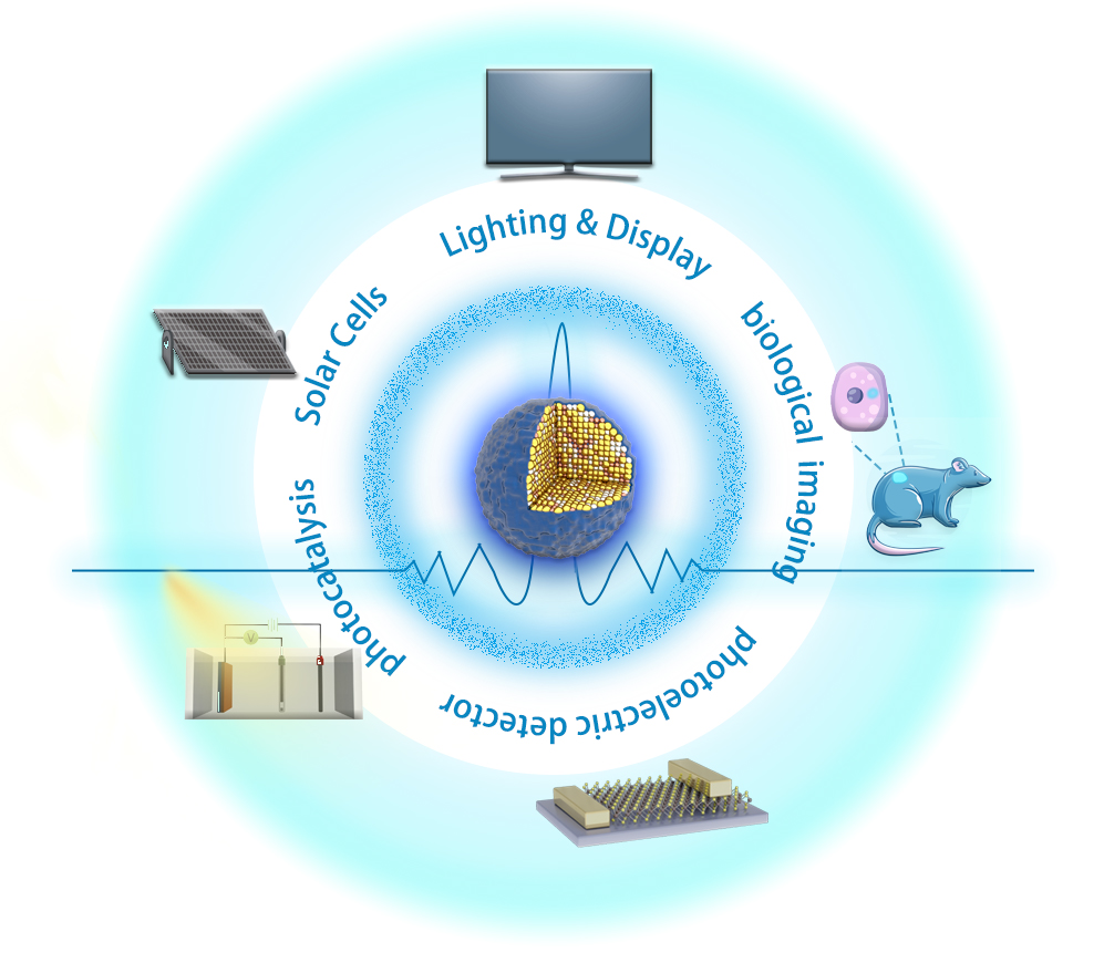
Quantum dots are considered as ideal luminescent materials for high color gamut,flexible,and large area display,medical devices,and the application of other fields,due to their unique photoelectric properties.Compared with the quantum dots of binaryⅡ-ⅥorⅢ-Ⅴgroup,the quantum dots of ternaryⅠ-Ⅲ-Ⅵ2group have significant advantages in terms of ecological and environmental friendliness without containing Cd or Pb elements,large Stokes shift with adjustable band gap,long-life luminescence,etc.Moreover,it is facile to obtain emission wavelength adjustable continuously from visible to near-infrared region by changing chemical elements ratio in the composition of singleⅠ-Ⅲ-Ⅵ2family.These characters make theⅠ-Ⅲ-Ⅵ2quantum dots have broad application prospects in the fields of light-emitting diodes,solar cells,photodetectors,biological imaging,etc.This paper systematically reviews the synthesis methods and optical performance optimization strategies of quantum dots and those suitable for I-III-VI2quantum dots,explains the luminescence mechanisms of I-III-VI2quantum dots based on their electronic band structures,summarizes recent-years progress of quantum dots application in lighting and display devices,and focuses on the application progress of the I-III-VI2quantum dots in photo-and electroluminescent diodes.Finally,the future prospects and challenges of I-III-VI2quantum dots are prospected 。
1 Introduction
2 Quantum dot synthesis method
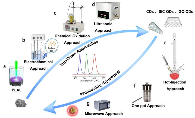
2.1 Top-down synthesis
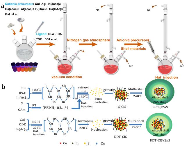
2.2 Bottom-up-heat injection method
2.3 Bottom-up-one-pot hot method
3 Current status of research based on groupⅠ-Ⅲ-Ⅵ2quantum dots
3.1 Luminescence mechanisms of groupⅠ-Ⅲ-Ⅵ2quantum dots
3.2 Optimization of optical properties of groupⅠ-Ⅲ-Ⅵ2quantum dots
4 GroupⅠ-Ⅲ-Ⅵ2quantum dot light emitting devices
4.1 Quantum dot luminescent display
4.2 GroupⅠ-Ⅲ-Ⅵ2quantum dot QLED and WLED devices
5 Conclusion and outlook
Fanghai Liu , Hui Jiang , Shuqi Yang , Qi Liu , Lei Chen . Preparation of GroupⅠ-Ⅲ-Ⅵ2 Quantum Dots and Light-Emitting Diode Devices[J]. Progress in Chemistry, 2024 , 36(7) : 1046 -1060 . DOI: 10.7536/PC231201
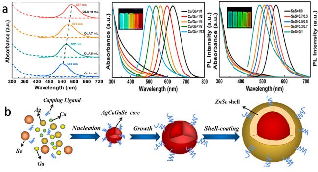
图3 (a)不同油氨剂量、前驱体比例、硫源掺杂CuGaSe2/ ZnSe量子点的紫外可见吸收光谱和光致发光谱[29];(b)Ag-Cu-Ga-Se多元量子点生长机理图[34]Fig 3 (a)UV-vis absorption spectra and photoluminescence spectra of CuGaSe2/ZnSe quantum dots doped with different oleoammonia doses, precursor ratios, and sulfur source[29]. (b)Ag-Cu-Ga-Se multiplexed quantum dot growth mechanism[34] |
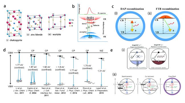
图4 (a)黄铜矿、闪锌矿和纤锌矿晶体结构[42];(b)Ⅰ-Ⅲ-Ⅵ2族量子点的电子能带结构和不同的重组或猝灭路径[37];(c)DAP重组和FTB重组示意图[14];(d)黄铜矿和纤锌矿CuInS2量子点的辐射衰变机制及观测到的能量[43];(e)俄歇复合导致Cu2+的PL猝灭,辐射复合导致Cu+的亮化;不缺铜和缺铜的CuInS2量子点以及CuInS2/ZnS 核壳结构的弛豫过程示意图[44,45]Fig. 4 (a)Crystal structures of chalcopyrite, sphalerite, and fibrillar zincite[42]. (b)Electronic energy band structures and different recombination or quenching paths of group Ⅰ-Ⅲ-Ⅵ2 quantum dots[37]. (c)Schematic diagrams of the DAP recombination and the FTB recombination[14]. (d)Overview of the radiative decay mechanisms of the CuInS2 quantum dots of chalcopyrite and fibrillar zincite and their observed energies[43]. (e)Rushes of composites leading to the PL burst of Cu2+ and radiative complexation leads to Cu+ brightening; schematic diagrams of the relaxation processes in Cu-less and Cu-deficient CuInS2 quantum dots as well as in the CuInS2/ZnS core-shell structure[44,45] |
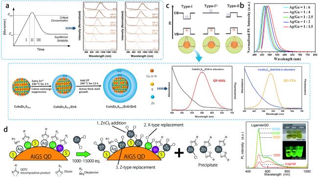
图5 (a)LaMer形核理论[62],CuInS2量子点吸光度和PL光谱演化[63];(b)不同Ag、Ga前驱体比例的PL光谱图[64];(c)核壳结构量子点中三种电荷载流子局域化机制的示意图[53], 多壳层CIZS/ZnS/ZnS量子点合成过程示意图和PL光谱[55];(d)配体交换机制的示意图[28]Fig 5 (a)LaMer shaped nucleus theory[62], CuInS2 quantum dots absorbance and PL spectral evolution[63]. (b)PL spectra of different Ag and Ga precursor ratios[64]. (c)Schematic representation of the three charge carrier localization mechanisms in the core-shell structured quantum dots[53]. Schematic representation of the synthesis process of the multi-shell CIZS/ZnS/ZnS quantum dots and PL spectra[55]. (d)Schematic representation of the ligand exchange mechanism[28] |
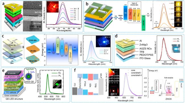
图6 (a)基于CuInS2/ZnS的QLED结构示意图,横截面TEM图像和器件的EL光谱随电压演化[85];(b)多壳层CuInS2/ZnS的QLED器件示意图,相应的能级图和器件的EL光谱随电压演化[86];(c)蓝光ZCGS、黄光CIS及其混合物的QLED结构,相应的能级图和器件的EL光谱随电压演化[58];(d)基于AGZS的QLED结构示意图结构和器件对应的EL光谱和PL光谱[59];(e)基于AIGS/GaS的QLED结构示意图,以及PL和EL光谱[88];(f)基于ZAIGS多元量子点的QLED结构示意图,核壳结构的EL光谱以及器件中载流子分布和复合的示意图[60]Fig. 6 (a)Schematic QLED structure based on CuInS2/ZnS, cross-sectional TEM image and EL spectra of the device evolving with voltage[85]. (b)Schematic QLED device based on multi-shell layer CuInS2/ZnS, corresponding energy level diagrams and EL spectra of the device evolving with voltage[86]. (c)QLED structure for blue ZCGS, yellow CIS and their mixtures, corresponding energy level diagrams and EL spectra of the devices evolving with voltage[58]. (d)Schematic structure of QLED based on AGZS Schematic structure and corresponding EL spectra and PL spectra of the devices[59]. (e)Schematic structure of QLED structure based on AIGS/GaS, along with the PL and EL spectra[88]. (f)Schematic structure of QLED structure based on ZAIGS multiplexed quantum dots, EL spectra of the core-shell structure, and the device Schematic representation of carrier distribution and complexation in the device[60] |
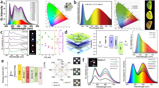
图7 (a)CIS量子点器件正向电流相关EL光谱演化以及CIE白光颜色坐标[92]; (b)在20 mA的驱动电流下,基于绿色和红色QD/PAAm膜的LED的发射光谱和CIE色坐标[93]; (c)CGS和CIS量子点之间的不同重量比制造白光WLED的EL光谱、CRI、CCT和发光效率的变化[95]; (d)基于单一体系CGS核壳量子点的WLED器件结构图和能带图,EL光谱随电压演化[96]; (e)In掺杂Zn-Cu-Ga-S/ZnS的WLED器件结构图、CRI的比例变化[97]; (f)双体系CIS和CGS核壳量子点混合发光层的WLED器件EL光谱以及归一化光谱随电压演化[58]Fig. 7 (a)Forward current-dependent EL spectral evolution of CIS quantum dot devices and CIE white light color coordinates[92]. (b)Emission spectra and CIE color coordinates of LED based on green and red QD/PAAm films at a drive current of 20 mA[93]. (c)Variation of EL spectra, CRI, CCT and luminous efficiency of white WLED fabricated with different weight ratios between CGS and CIS quantum dots[95]. (d)Structural and energy band diagrams of WLED devices based on single-system CGS core-shell quantum dots, EL spectra evolution with voltage[96]. (e)Structure of In-doped Zn-Cu-Ga-S@ZnS WLED device, scale variation of CRI[97]. (f)EL spectra of WLED devices with dual-system CIS and CGS core-shell quantum dots hybrid light-emitting layers and normalized spectra evolution with voltage[58] |
| [1] |
García de Arquer F P,
|
| [2] |
|
| [3] |
|
| [4] |
|
| [5] |
|
| [6] |
|
| [7] |
|
| [8] |
|
| [9] |
|
| [10] |
|
| [11] |
|
| [12] |
|
| [13] |
|
| [14] |
|
| [15] |
|
| [16] |
|
| [17] |
|
| [18] |
|
| [19] |
|
| [20] |
|
| [21] |
|
| [22] |
|
| [23] |
|
| [24] |
|
| [25] |
|
| [26] |
|
| [27] |
|
| [28] |
|
| [29] |
|
| [30] |
|
| [31] |
|
| [32] |
|
| [33] |
|
| [34] |
|
| [35] |
|
| [36] |
|
| [37] |
|
| [38] |
|
| [39] |
|
| [40] |
|
| [41] |
|
| [42] |
|
| [43] |
|
| [44] |
|
| [45] |
|
| [46] |
|
| [47] |
|
| [48] |
|
| [49] |
|
| [50] |
|
| [51] |
|
| [52] |
|
| [53] |
|
| [54] |
|
| [55] |
|
| [56] |
|
| [57] |
|
| [58] |
|
| [59] |
|
| [60] |
|
| [61] |
|
| [62] |
|
| [63] |
|
| [64] |
|
| [65] |
|
| [66] |
|
| [67] |
|
| [68] |
|
| [69] |
|
| [70] |
|
| [71] |
|
| [72] |
|
| [73] |
|
| [74] |
|
| [75] |
|
| [76] |
|
| [77] |
|
| [78] |
|
| [79] |
|
| [80] |
|
| [81] |
|
| [82] |
|
| [83] |
|
| [84] |
|
| [85] |
|
| [86] |
|
| [87] |
|
| [88] |
|
| [89] |
|
| [90] |
|
| [91] |
|
| [92] |
|
| [93] |
|
| [94] |
|
| [95] |
|
| [96] |
|
| [97] |
|
| [98] |
|
/
| 〈 |
|
〉 |