
Raman Spectroscopy in the Detection of Environmental Micro- and Nanoplastics: Applications and Challenges
Received date: 2024-07-10
Revised date: 2024-08-26
Online published: 2025-01-20
Supported by
National Natural Science Foundation of China(22241601)
This review highlights the advantages and research advancements of Raman spectroscopy in detecting micro- and nanoplastics in the environment. With the worsening issue of microplastic pollution, particularly its widespread presence in aquatic and terrestrial ecosystems, Raman spectroscopy has emerged as a non-destructive, high-resolution analytical technique widely employed for identifying and quantitatively analyzing micro- and nanoplastics. This is attributed to its unique spectral characteristics and reduced susceptibility to water interference compared to infrared spectroscopy. The strengths of Raman spectroscopy in detecting micro- and nanoplastics lie in its high spatial resolution, broad spectral range, and exceptional sensitivity. However, challenges such as fluorescence interference and low signal-to-noise ratios persist in the detection process. To enhance Raman signals, researchers have introduced various approaches, including sample pretreatment, surface-enhanced Raman spectroscopy (SERS), and nonlinear Raman spectroscopy techniques. Furthermore, this paper underscores the necessity of building a comprehensive Raman spectroscopy database to boost detection accuracy and efficiency. Future research directions include developing more effective preprocessing methods, dynamically monitoring the behavior of micro- and nanoplastics, and integrating intelligent detection systems.
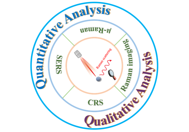
1 Introduction
2 Raman spectroscopy methods for micro-and nanoplastics
2.1 Basic principles and conventional Raman spectroscopy
2.2 Surface-enhanced Raman spectroscopy (SERS)
2.3 Coherent Raman spectroscopy (CRS)
2.4 Raman imaging
3 Identification in environmental samples with Raman spectroscopy
3.1 Fluorescence interference and its elimination
3.2 Machine learning applications with Raman spectral databases
4 Quantitative Analysis
4.1 In situ concentration and mass concentration
4.2 Number concentration via µ-Raman and imaging
5 Conclusion and outlook
Kefu Ye , Minjie Xie , Xingqi Chen , Zhiyu Zhu , Shixiang Gao . Raman Spectroscopy in the Detection of Environmental Micro- and Nanoplastics: Applications and Challenges[J]. Progress in Chemistry, 2025 , 37(1) : 2 -15 . DOI: 10.7536/PC240710
Figure 1 (a) A "coffee ring" was formed on the surface enhanced substrate of klarite; (b) Schematic diagram of enhanced Raman signal on colloidal surface of metal nanoparticles; (c) Two kinds of coherent Raman spectrum mechanism diagrams; (d) Schematic diagram of Raman spectral imagingFig. 1 (a) Schematic diagram of the formation of “coffee ring” on Klarite surface-enhanced substrates ;(b) Schematic diagram of the colloidal surface-enhanced Raman signals of metal nanoparticles; (c) Mechanism of the two coherent Raman spectra; (d) Schematic diagram of Raman spectroscopic imaging |
Table 1 Application of metal nano array substrate in the detection of micro nano plasticsTable 1 The application of metal nanoarray substrates in the detection of micro- and nanoplastics |
| Class | SERS material or structure | Target | Dispersed System | Limit of detection | Excitation wavelength | ref | |
|---|---|---|---|---|---|---|---|
| Non-membrance pattern | Klarite | PS, PMMA≥360 nm | Pure water | Single nanoplastic | 785 nm | 35 | |
| PET, PMMA≥450 nm | Atmospheric Aerosols | ||||||
| SiO2 PC@Ag | PS 100~1000 nm | Pure water | Single nanoplastic | 633 nm | 36 | ||
| Bottled, river, and tap water spiked samlpes | 5 µg/g | ||||||
| AAO/MoS2/Ag | PS 100~300 nm | Pure water | - | 532 nm | 37 | ||
| Au/Ag triangular cavity array | PS 50~1000 nm | Pure water | 10 µg/g | 532 nm | 38 | ||
| PET 88.2 nm | Bottled water | - | |||||
| Ag/ZnO@PDMS | PS 800 nm | Pure water | 25 µg/mL | 785 nm | 39 | ||
| Spiked samples of tap water, lake water, river water, seawater | Tap water 25 µg/mL;lake water 28 µg/mL;river water 35 µg/mL; Seawater 60 µg/mL | ||||||
| Non-membrance pattern | AuNPs@V-shaped AAO | PS, PMMA≥1 µm | Pure water | Single particle | 785 nm | 40 | |
| PS≥2 µm | Spiked samples of rain water | ||||||
| Au nanoparticles self-assembled on a glass slide | PS 161 nm; 33 nm PET 62 nm | Pure water | PS 10 µg/mL PET 15 µg/mL | 785 nm | 32 | ||
| Silver-coated gold nanostars inserted into anodized aluminum oxide (AAO) nanopore | PS≥400 nm | Pure water | 50 µg/mL | 633 nm | 41 | ||
| Spiked samples of tap water, river water and seawater | 500 µg/mL | ||||||
| Membrane pattern | Gold nanorods assembled on cellulose | PS 84 nm;630 nm | Pure water | 100 µg/mL | 785 nm | 42 | |
| Au-AAO membrance | PS 360 nm, 500 nm, 1 µm, 2 µm, 5 µm; PMMA 360 nm, 500 nm, 2 µm, 5 µm | Pure water | Single particle | 785 nm | 43 | ||
| PS PE≥360 nm | Sea salt | ||||||
| Au nanoparticles self-assembled on filter paper | PET≥20 µm | Pure water | 100 µg/mL | 532 nm | 44 | ||
| Spiked samples of tap water and pool water | |||||||
| Self-assembly of spiked Au nanoparticles on glass fiber filter membrane | PS 20~10000 nm | Pure water | 0.1 µg/mL | 785 nm | 45 | ||
| Spiked samples of tap water and rain water | |||||||
| Silver Nanowire Membrane | PS 50~1000 nm | Pure water | 10-3 µg/mL | 785 nm | 46 | ||
| seawater | - | ||||||
Table 2 Application of metal nanoparticles colloid in the detection of micro nano plasticsTable 2 The application of metal nanoparticle colloids in the detection of micro- and nanoplastics |
| SERS material | Target | Dispersed System | Limit of detection | Excitation wavelength | Detection environment | Ref |
|---|---|---|---|---|---|---|
| Ag nanoparticles solution | PS 20~5000 nm | Pure water | 5 µg/mL | 785 nm | Direct determination in solution | 47 |
| Spiked samples of rain water and bottled water | ||||||
| Ag nanoparticles solution | PS≥100 nm | Pure water | 40 µg/mL | 785 nm | 34 | |
| Spiked of seawater | 40 µg/mL | |||||
| Ag nanoparticles solution | PS 50~500 nm | Pure water | 6.25 µg/mL | 785 nm | 48 | |
| Spiked of lake water | - | |||||
| Ag nanoparticles | PS 20 nm | Pure water | 10 µg/mL | 785 nm | Drying after mixing | 49 |
| CuO/Ag nanoparticles | PE 400 µm | Pure water | 1.6 ng/mL | 532 nm | 50 | |
| Au nanourchins | PS 600 nm | Pure water | - | 785 nm | 51 |
Table 3 An algorithm for transforming hyperspectral signals in Raman imaging analysis of micro/nano plasticsTable 3 Algorithm for transforming hyperspectral signals in Raman imaging analysis of micro- and nanoplastics. |
| Class | Algorithm | Advantages | Disadvantages | Ref |
|---|---|---|---|---|
| Threshold determination | Otsu's algorithm | Automatic, simple, and fast identification Applicable to both bright field and dark field microscopy Suitable for different particle sizes, shapes, colors, and transparency | Insensitive to contrast between particles and background Unable to distinguish fibers from aggregates | 82 |
| Multi-image merging | Logic-based | Cross-validation of different characteristic peak signals Effectively shields interference signals High accuracy in mapping | Complex processing workflow | 79 |
| Algebraic | Algebra-based | High computational flexibility Ability to integrate with other algorithms | Failure to consider varying contributions of different peaks Potential signal loss issues | 83 |
| Multivariate | Principal Component Analysis(PCA) | Effective extraction of critical information Independent of standard Raman spectra | Significant background interference Lower accuracy | 84 |
| PCA-linear discriminant analysis | Automatic identification of polymer types High accuracy in identifying plastic types Applicable to aged microplastics | Issues with signal loss Mismatch in feature changes | 85 | |
| Dual-PCA | High signal-to-noise ratio imaging Automatic classification of various polymers Suitable for machine learning | High computational complexity Difficulty in feature selection | 81 | |
| Multivariate curve resolution-alternating least squares | Analysis in complex backgrounds Samples require no pre-processing | Dependent on constraints High sensitivity to data noise | 86 |
Figure 2 (a) Schematic diagram of fluorescence interference and suppression technology; (b) Schematic diagram of Raman spectrum recognition processing of micro nano plastics in environmental samples through machine learningFig. 2 (a) Schematic diagram of fluorescence interference and suppressed fluorescence techniques; (b) Schematic diagram of Raman spectral recognition processing of micro- and nanoplastics in environmental samples by machine learning. |
| [1] |
|
| [2] |
|
| [3] |
|
| [4] |
|
| [5] |
|
| [6] |
|
| [7] |
|
| [8] |
|
| [9] |
|
| [10] |
|
| [11] |
|
| [12] |
|
| [13] |
|
| [14] |
|
| [15] |
|
| [16] |
|
| [17] |
|
| [18] |
|
| [19] |
|
| [20] |
|
| [21] |
|
| [22] |
|
| [23] |
|
| [24] |
|
| [25] |
|
| [26] |
|
| [27] |
|
| [28] |
|
| [29] |
|
| [30] |
|
| [31] |
|
| [32] |
|
| [33] |
|
| [34] |
|
| [35] |
|
| [36] |
|
| [37] |
|
| [38] |
|
| [39] |
|
| [40] |
|
| [41] |
|
| [42] |
|
| [43] |
|
| [44] |
|
| [45] |
|
| [46] |
|
| [47] |
|
| [48] |
|
| [49] |
|
| [50] |
|
| [51] |
|
| [52] |
|
| [53] |
|
| [54] |
|
| [55] |
|
| [56] |
|
| [57] |
|
| [58] |
|
| [59] |
|
| [60] |
|
| [61] |
|
| [62] |
|
| [63] |
|
| [64] |
|
| [65] |
|
| [66] |
|
| [67] |
|
| [68] |
|
| [69] |
|
| [70] |
|
| [71] |
|
| [72] |
|
| [73] |
|
| [74] |
|
| [75] |
|
| [76] |
|
| [77] |
|
| [78] |
|
| [79] |
|
| [80] |
|
| [81] |
|
| [82] |
|
| [83] |
|
| [84] |
|
| [85] |
|
| [86] |
|
| [87] |
|
| [88] |
|
| [89] |
|
| [90] |
|
| [91] |
|
| [92] |
|
| [93] |
|
| [94] |
|
| [95] |
|
| [96] |
|
| [97] |
|
| [98] |
|
| [99] |
|
| [100] |
|
| [101] |
|
| [102] |
|
| [103] |
|
| [104] |
|
| [105] |
|
| [106] |
|
| [107] |
|
| [108] |
|
| [109] |
|
| [110] |
|
| [111] |
|
| [112] |
|
| [113] |
|
| [114] |
|
| [115] |
|
| [116] |
|
| [117] |
|
| [118] |
|
| [119] |
|
| [120] |
|
| [121] |
|
/
| 〈 |
|
〉 |

