
Interlayer Spacing Regulations on MoS2-Based Supercapacitors: Recent Advances and Challenges
Received date: 2025-06-09
Revised date: 2025-06-26
Online published: 2025-07-15
Supported by
The Xinjiang Uygur Automomous Region Science and Technology Plan Project-Key R&D Special Project(2022B02051)
The Semiconductor physics and micro and nano devices Tianshan Innovation team(2023D14001)
The Tianshan Talent Training Project-Xinjiang Science and Technology Innovation Team Program(2023TSYCTD0012)
Due to its unique layered structure and excellent electrochemical properties, molybdenum disulfide (MoS2) demonstrates significant potential for applications in the energy storage field, particularly in supercapacitors. It is widely regarded as one of the most representative transition metal dichalcogenides. MoS2 possesses a high theoretical specific capacitance, abundant edge active sites, and favorable tunability and structural diversity, which provide it with a distinct advantage in the construction of advanced electrode structures. Additionally, the anisotropic characteristics of MoS2 concerning electron and ion transport offer more dimensions for regulating its electrochemical behavior. This work will systematically review various synthesis strategies for MoS2 and its recent advancements in energy storage, with a particular focus on the mechanisms by which interlayer spacing modulation affects energy storage behavior in supercapacitor configurations. The discussion will encompass a comprehensive logical framework that spans material structure modifications, electronic configuration evolution, and enhancements in macroscopic device performance. This review aims to provide theoretical support and practical guidance for the application of MoS2 in the next generation of high-performance energy storage devices.
1 Introduction
2 Overview of MoS2 as a fundamental electrode material for supercapacitors
3 Synthesis strategies of MoS2
3.1 “Bottom-up” synthesis of MoS2
3.2 “Top-down” synthesis of MoS2
4 Strategy of modulating MoS2 interlayer spacing and the effects on electrochemical properties
4.1 Interlayer agent induces interlayer spacing expansion
4.2 3D structure construction
4.3 Defect engineering
4.4 Other methods to regulate the interlayer spacing of MoS2
4.5 Theoretical understanding
5 Summary and outlook
Wu Mingyu , Ma Dongliang , Hua Qingsong , Lu Shun . Interlayer Spacing Regulations on MoS2-Based Supercapacitors: Recent Advances and Challenges[J]. Progress in Chemistry, 2025 , 37(9) : 1235 -1260 . DOI: 10.7536/PC20250605
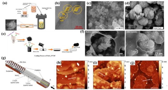
图3 (a) MoS2的合成,(b) HRTEM[71];(c, d) 不同反应时间下产物的SEM[72];(e) 1T/2H MoS2 PVDF的合成示意图,(f) FESEM[76];(g) 在不同衬底上生长MoS2的AFM图:(h) 蓝宝石,(i) 石墨烯,(j) SiO2[83]Fig.3 (a) Preparation process of MoS2. (b) HRTEM. Reproduced with permission from Ref 71. Copyright 2022 Elsevier. (c, d) SEM analysis of products under different reaction times. Reproduced with permission from Ref 72. Copyright 2015 Elsevier. (e) Schematic representation of the synthesis of 1T/2H MoS2-PVDF. (f) FESEM. Reproduced with permission from Ref 76. Copyright 2022 Elsevier. (g) AFM images of MoS2 growth on different substrates: (h) sapphire; (i) graphene; (j) SiO2. Reproduced from Ref 83. Copyright 2020 American Chemical Society |
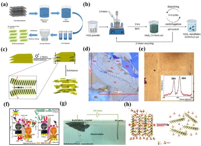
图4 (a) LPE法合成MoS2 [84];(b) 2-MeIm辅助剥离流程,(c) MoS2剥离机制[85];(d, e) 光学显微图像[86];(f) MSLDH3电荷转移路径[87];(g)电化学剥离的实验装置,(h)剥落过程示意图[88]Fig.4 (a) LPE synthesis of MoS2. Reproduced from Ref 84. Copyright 2020 American Chemical Society. (b) 2-MeIm assisted process, (c) exfoliation mechanism of MoS2. Reproduced with permission from Ref 85. Copyright 2022 Elsevier. (d, e) Optical microscope images. Reproduced with permission from Ref 86. Available under CC-BY 4.0. Copyright 2015 The Authors. (f) Charge transfer path in MSLDH3. Reproduced from Ref 87. Copyright 2019 American Chemical Society. (g) Electrochemical exfoliation setup of MoS2; (h) exfoliation process. Reproduced with permission from Ref 88. Copyright 2014 Elsevier |
表1 各种原位合成方法的优缺点Table 1 Advantages and disadvantages of various in situ synthesis methods |
| Synthesis methods | Advantages | Disadvantages |
|---|---|---|
| Hydrothermal method | Suitable for thermally unstable materials. Controllable morphology and structure. Green, scalable synthesis. | High equipment cost and safety risks. Limited process visibility and difficult control. Long reaction time and high energy consumption. |
| Solvothermal method | Precise morphology control. Low contamination risk. High surface area, low aggregation. | Solvent impurities. Purity issues due to residues. Not for high-melting/insoluble precursors. |
| Chemical vapor deposition | High-quality crystals. Controllable size and thickness. Large-area compatibility. | High cost. Limited morphology control. Complex and time-consuming process. |
| Liquid phase exfoliation method | Low-cost and scalable. Simple process. High yield. | Safety risks. Low quality control. Restacking and degradation. |
| Solid phase exfoliation | Highest quality. Simple and clean. Ideal for fundamental research. | Extremely low yield. Uncontrollable morphology. Substrate limitation. |
| Electrochemical exfoliation method | High yield & low cost. Large flake size. Scalable and continuous production. | Limited property control. Chemical instability risk. Process complexity |
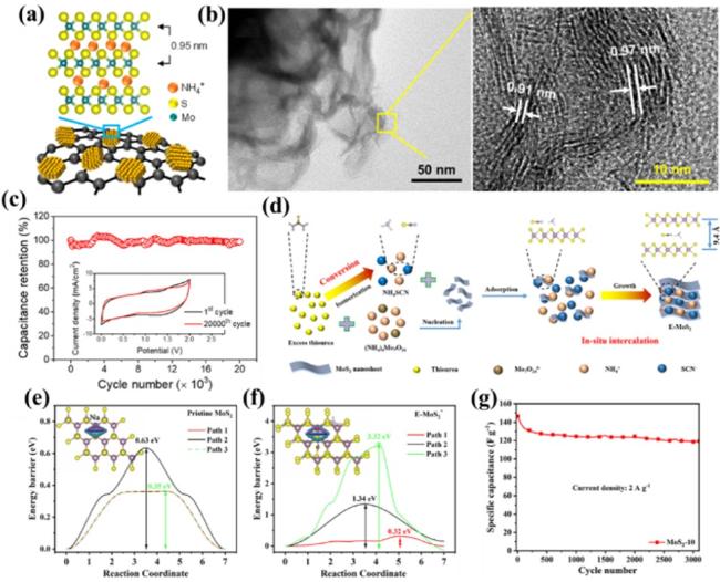
图5 (a) NH4+插层MoS2,(b) SEM和TEM,(c) 循环稳定性[34];(d) 层间膨胀MoS2合成路线,(e) Na+迁移能垒,(f) E-MoS2的离子扩散;(g) 稳定性[89]Fig.5 (a) NH4+ intercalation in MoS2, (b) SEM and TEM, (c) cycling stability. Reproduced from Ref 34. Copyright 2019 American Chemical Society. (d) Synthesis route for expanded MoS2, (e) Na⁺ migration barrier, (f) ion diffusion in E-MoS2, (g) stability test. Reproduced with permission from Ref 89. Copyright 2023 Royal Society of Chemistry |
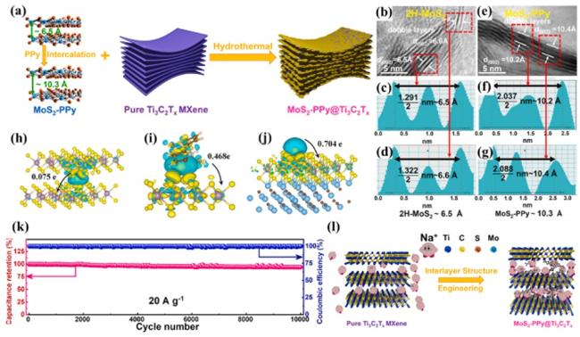
图6 (a) MoS2-PPy@Ti3C2Tx的结构图,2H-MoS2(b~d)与MoS2-PPy(e~g)的HRTEM图,(h) MoS2-Na电荷差侧视图;(i) MoS2-PPy-Na电荷差侧视图;(j) MoS2/MXene-Na电荷差侧视图,(k) 电极的电容保持率和库仑效率,(l) 混合材料中层间结构的调节机制[90]Fig.6 (a) Schematic illustration of the architecture of the MoS2-PPy@Ti3C2Tx, HR-TEM images of the 2H-MoS2 (b~d) and MoS2-PPy (e~g), (h) side view of charge density difference for MoS2-Na; (i) side view of charge density difference for MoS2-PPy-Na; (g) side view of charge density difference for MoS2/MXene-Na. Reproduced with permission from Ref 90. Copyright 2025 Elsevier |
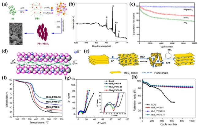
图7 (a) PPy/MoS2的制备流程,(b) PPy/MoS2的全测量光谱,(c) 循环性能测试,(d) 电子传输示意图[91];(e) 实验方法示意图,(f) PANI/MoS2/PANI的TGA曲线,(g)奈奎斯特曲线,(h)循环稳定性测试[92]Fig.7 (a) Schematic illustration for the fabrication of PPy/MoS2, (b) full survey spectrum of PPy/MoS2, (c) cycling performance, (d) schematic of the electron transportation. Reproduced with permission from Ref 91. Copyright 2017 Elsevier. (e) Schematic presentation of the experimental method, (f) TGA curve of PANI/MoS2/PANI, (g) Nyquist plots, (h) cycle stability testing of composite materials. Reproduced with permission from Ref 92. Copyright 2015 Elsevier |
图8 (a) MoS2/NiCoHC示意图,(b) SEM,(c) 循环稳定性[94];(d) 3D MoS2/C@RGO生长机制,(e,f) TEM;(g) 循环稳定性[95];(h,i) MoS2的FESEM图,(j, k) KCL/KOH电解质稳定性测试[96]Fig.8 (a) Synthesis of MoS2/NiCoHC, (b) SEM, (c) cycle stability. Reproduced with permission from Ref 94, Copyright 2021 Elsevier. (d) Growth mechanism of 3D MoS2/C@RGO, (e, f) TEM, (g) cycle stability. Reproduced with permission from Ref 95, Copyright 2019 Elsevier. (h,i) FESEM of MoS2, (j, k) stability tests in KCL/KOH electrolytes. Reproduced from Ref 96. Copyright 2019 American Chemical Society |
图9 (a) 合成MoS2@CNT电极示意图,(b) HRTEM图,(c, d) CNT水接触角,(e) GCD曲线,(f) 循环2500次后的GCD曲线[97];(g) MoS2/PEDOT:PSS/CNTs薄膜合成图,(h) TEM,(i) HAADF-STEM,(j) MoS2@C/CNTs的结构示意图,(k) GCD曲线,(l)电容保持率及库仑效率[98]Fig.9 (a) Synthesis of MoS2@CNT electrode, (b) HRTEM, (c, d) water contact angle of CNT, (e) GCD curves, (f) GCD curve after 2500 cycles. Reproduced with permission from Ref 97. Copyright 2019 Elsevier. (g) Synthesis of MoS2/PEDOT:PSS/CNTs film, (h) TEM, (i) HAADF-STEM, (j) structure of MoS2@C/CNTs, (k) GCD curves, (l) capacitance retention and coulombic efficiency. Reproduced with permission from Ref 98. Copyright 2020 Elsevier. |
图10 (a) 金属掺杂MoS2纳米结构,(b, c) Cu-MoS2 的FESEM,(d) 原始和掺杂的MoS2比电容的对比,(e) 循环稳定性[107];(f) 样品示意图,(g, h) S-Ⅱ的HRTEM图,(i, j) S-Ⅰ和S-Ⅱ的电容值,(k) S-Ⅰ/S-Ⅱ CV电容(左)与GCD电容(右),(l) 器件点亮LED展示[108]Fig.10 (a) Metal-doped MoS2 nanostructures; (b, c) FESEM of Cu-MoS2, (d) specific capacitance comparison: pure vs. doped MoS2, (e) cycling stability. Reproduced with permission from Ref 107. Copyright 2022 Elsevier. (f) Scheme of sample structure, (g, h) HRTEM of S-Ⅱ, (i, j) capacitance values: S-Ⅰ/S-Ⅱ; (k) CV capacitance (left) and GCD capacitance (right) for S-Ⅰ/S-Ⅱ; (l) device powering LEDs. Reproduced with permission from Ref 108. Copyright 2020 Elsevier |
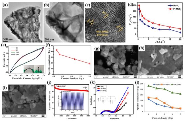
图11 (a,b) Pt掺杂MoS2的TEM,(c) HRTEM图,(d) 比电容与电流密度的关系;(e) 100 ℃不同弯曲角度下的CV曲线,(f) 不同电流密度下的比电容[109];(g) MoS2, (h) Nd-MoS2和(i) Gd-MoS2的SEM图,(j) Gd-MoS2的循环稳定性,(k) 奈奎斯特图,(l) 比电容与电流密度的关系[110]Fig.11 (a, b) TEM image of Pt-doped MoS2, (c) HRTEM, (d) relationship between specific capacitance and current density, (e) CV curves at different bending angles at 100 ℃, (f) specific capacitance at different current densities. Reproduced with permission from Ref 109. Copyright 2019 Elsevier. SEM images of pure (g) MoS2, (h) Nd-MoS2 and (i) Gd-MoS2, (j) cycling stability of Gd-MoS2, (k) Nyquist plot, (l) relationship between specific capacitance and current density. Reproduced from Ref 110. Copyright 2022 American Chemical Society |
图12 (a) 制备具有内在缺陷的MoS2,(b) HRTEM图,(c) HRTEM图,(d) 用巯基乙酸钠合成的MoS2的FESEM图像[111];(e) MoS2-x-300(f)MoS2-x-500(g)MoS2-x-700的HRTEM图,(h) 循环稳定性,(i) 无缺陷MoS2和含有三种原子空位的MoS2-x的示意图[113]Fig.12 (a) Preparation of MoS2 with intrinsic defects; (b) HRTEM of edge, (c) HRTEM; (d) FESEM image of MoS2. Reproduced with permission from Ref. [111]. Copyright 2015 Royal Society of Chemistry. (e) HRTEM of MoS2-x-300 (f), MoS2-x-500 (g), MoS2-x-700; (h) cycling stability; (i) schematic diagram of defect-free MoS2 and MoS2-x containing three types of atomic vacancies. Reproduced with permission from Ref 113. Available under CC-BY-NC 3.0. Copyright 2021 The Authors |
表2 MoS2复合材料调控方法的性能比较Table 2 Comparison of regulation methods for MoS2 composite materials |
| Interlayer spacing | Material | Capacitance | Number of cycles | Ref |
|---|---|---|---|---|
| 0.95 nm | MoS2/r-GO//Fe2O3/MnO2 | 1.54 F·cm-3 | Retention rate 98% after 20 000 cycles | 34 |
| 9.4 Å | MoS2-10 | 476.0 F·g-1 | Retention rate 81.7% after 3000 cycles | 89 |
| 10.3 Å | MoS2-PPy@Ti3C2TxMXene | 265 F·g-1 | Retention rate 94.1% after 10 000 cycles | 90 |
| 0.63 nm | PPy/MoS2 | 895.6 F·g-1 | Retention rate 98% after 10 000 cycles | 91 |
| 0.63 nm | MoS2@CNT | 337 mF·cm-2 | Retention rate 97.8% after 2500 cycles | 97 |
| 0.72 nm | MoS2@C/CNTs | 335 F·g-1 | Retention rate 127% after 40 000 cycles | 98 |
| 0.76 nm | low Mn-doping (S-Ⅱ) | 88 F·g-1 | Retention rate 77% after 5000 cycles | 108 |
| 0.65 nm | Pt dope MoS2 | 250 F·g-1 | Retention rate 88% after 3000 cycles | 109 |
| 0.62 nm | defect-rich MoS2 | 270.3 F·g-1 | Retention rate 91.2% after 2000 cycles | 111 |
| 0.625 nm | HDD-MoS2 | 379 F·g-1 | Retention rate 92% after 3000 cycles | 112 |
| 0.628 nm | MoS2-x-700 | 142.3 F·g-1 | Retention rate 87.1% after 5000 cycles | 113 |
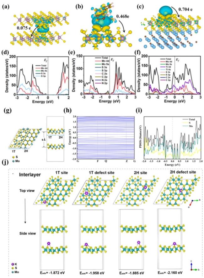
图13 (a) MoS2-Na电荷差侧视图;(b) MoS2-PPy-Na电荷差侧视图;(c) MoS2/MXene-Na电荷差侧视图,(d) MoS2,(e) MoS2-PPy和(f)MoS2的态密度[90];(g) MoS2模型结构,(h) MoS2模型的能带,(i) 状态密度,(j) MoS2在层间的吸附模型[115]Fig.13 (a) Side view of charge density difference for MoS2-Na; (b) side view of charge density difference for MoS2-PPy-Na; (c) side view of charge density difference for MoS2/MXene-Na, density of states for model (d) MoS2, (e) MoS2-PPy and (f) MoS2. Reproduced with permission from Ref 90. Copyright 2025 Elsevier. (g) MoS2 model structure, (h) the energy band of the MoS2 model, (i) state density, (j) the adsorption models of MoS2 at the interlayer. Reproduced with permission from Ref 115. Copyright 2024 Elsevier |
图14 (a, b) MoS2与Ni- MoS2优化构型对比;(c) 总态密度(黑:原始,红:掺镍);(d) 原始MoS2PDOS;(e)原始能带结构;(f) Ni-MoS2 PDOS;(g) Ni-MoS2能带结构[116];(h) 电荷密度图MS@TeMS的等值线为0.052e,(i) 量子电容变化MS@Te和MS,(j) 总态密度,(k) Mo 4d的部分态密度[117]Fig.14 (a, b) Optimized geometries of MoS2 vs. Ni-MoS2, (c) total density of states (Black: Pure, Red: Ni-doped), (d) PDOS of pure MoS2, (e) band structure of pure MoS2, (f) PDOS of Ni-MoS2, (g) band structure of Ni-MoS2. Reproduced with permission from Ref 116. Copyright 2023 Elsevier. (h) Charge density isosurface (0.052e) of MS@TeMS; (i) quantum capacitance (Cq) variation: MS@Te vs. MS; (j) total density of states; (k) Mo 4d partial density of states. Reproduced with permission from Ref 117. Copyright 2023 Elsevier |
| [1] |
|
| [2] |
|
| [3] |
|
| [4] |
|
| [5] |
Heydari Gharahcheshmeh M,
|
| [6] |
|
| [7] |
|
| [8] |
( 吴云鹏, 王晓峰, 李本仙, 赵旭东, 刘晓旸. 化学进展, 2023, 35(7): 1005).
|
| [9] |
|
| [10] |
|
| [11] |
|
| [12] |
( 戚琦, 徐佩珠, 田志东, 孙伟, 刘杨杰, 胡翔. 化学进展, 2022, 34(9): 2051).
|
| [13] |
|
| [14] |
|
| [15] |
|
| [16] |
|
| [17] |
( 陈星, 蒋德敏, 谢昆, 刘丽君, 王堙, 王育乔. 化学进展, 2024, 36(7): 961).
|
| [18] |
|
| [19] |
|
| [20] |
|
| [21] |
|
| [22] |
|
| [23] |
|
| [24] |
|
| [25] |
|
| [26] |
|
| [27] |
|
| [28] |
|
| [29] |
|
| [30] |
|
| [31] |
|
| [32] |
|
| [33] |
|
| [34] |
|
| [35] |
|
| [36] |
|
| [37] |
|
| [38] |
|
| [39] |
|
| [40] |
|
| [41] |
|
| [42] |
|
| [43] |
|
| [44] |
|
| [45] |
|
| [46] |
|
| [47] |
|
| [48] |
|
| [49] |
|
| [50] |
|
| [51] |
|
| [52] |
|
| [53] |
|
| [54] |
|
| [55] |
|
| [56] |
|
| [57] |
|
| [58] |
|
| [59] |
|
| [60] |
|
| [61] |
|
| [62] |
|
| [63] |
|
| [64] |
|
| [65] |
|
| [66] |
|
| [67] |
|
| [68] |
|
| [69] |
|
| [70] |
|
| [71] |
|
| [72] |
|
| [73] |
|
| [74] |
|
| [75] |
|
| [76] |
|
| [77] |
|
| [78] |
|
| [79] |
|
| [80] |
|
| [81] |
|
| [82] |
|
| [83] |
|
| [84] |
|
| [85] |
|
| [86] |
|
| [87] |
|
| [88] |
|
| [89] |
|
| [90] |
|
| [91] |
|
| [92] |
|
| [93] |
|
| [94] |
|
| [95] |
|
| [96] |
|
| [97] |
|
| [98] |
|
| [99] |
|
| [100] |
|
| [101] |
|
| [102] |
|
| [103] |
|
| [104] |
|
| [105] |
|
| [106] |
|
| [107] |
|
| [108] |
|
| [109] |
|
| [110] |
|
| [111] |
|
| [112] |
|
| [113] |
|
| [114] |
|
| [115] |
|
| [116] |
|
| [117] |
|
/
| 〈 |
|
〉 |


