Home Journals Progress in Chemistry
Progress in Chemistry

Abbreviation (ISO4): Prog Chem      Editor in chief: Jincai ZHAO

About  /  Aim & scope  /  Editorial board  /  Indexed  /  Contact  / 
Review

Photovoltaic Cells Based on Carbon Nanotubes

  • Wang Long 1, 2 ,
  • Zhou Qingping 2 ,
  • Wu Zhaofeng 1 ,
  • Zhang Yanming 2 ,
  • Ye Xiaowo 2 ,
  • Chen Changxin , 1, 2, *
Expand
  • 1. School of Physics Science and Technology, Xinjiang University,Urumqi 830046, China
  • 2. National Key Laboratory of Science and Technology on Micro/Nano Fabrication, Key Laboratory for Thin Film Fabrication of the Ministry of Education, Department of Micro/Nano Electronics, School of Electronic Information and Electrical Engineering, Shanghai Jiao Tong University, Shanghai 200240, China
* Corresponding author e-mail:

These authors contributed equally to this work.

Received date: 2022-11-08

  Revised date: 2023-01-03

  Online published: 2023-02-16

Supported by

National Natural Science Foundation of China for Excellent Young Scholars(61622404)

National Natural Science Foundation of China(62074098)

Chang Jiang (Cheung Kong) Scholars Program of Ministry of Education of China(Q2017081)

Project from Zhejiang Fulai New Materials Co., Ltd.

Abstract

Carbon nanotubes (CNTs) are ideal materials for building photovoltaic cells due to their unique one-dimensional structure and excellent photoelectric properties. In this paper, we review recent structural design, fabrication method and device performance of CNT-based photovoltaic cells and different functional roles of CNTs in these devices. Firstly, the structure and photoelectric properties of CNTs are introduced. Then, we emphatically discuss the operation principles, the fabrication methods and the advantages and shortage of the photovoltaic cells with CNTs used as the photoelectric conversion materials, conducting electrodes and carrier transport layers in the devices. The applications of carbon nanotubes in Micro photovoltaic cell,carbon nanotube/silicon heterojunction photovoltaic cells, dye sensitized photovoltaic cells, perovskite photovoltaic cells, organic photovoltaic cells and flexible photovoltaic cells are introduced. Finally, the advantages and challenges of CNT-based photovoltaic cells are summarized. This paper will provide new idea and reference for the design and fabrication of novel carbon-based photovoltaic cells.

Cite this article

Wang Long , Zhou Qingping , Wu Zhaofeng , Zhang Yanming , Ye Xiaowo , Chen Changxin . Photovoltaic Cells Based on Carbon Nanotubes[J]. Progress in Chemistry, 2023 , 35(3) : 421 -432 . DOI: 10.7536/PC221106

Contents

1 Introduction
2 Structure and properties of carbon nanotubes
2.1 Structure of carbon nanotubes
2.2 Photoelectric properties of carbon nanotubes
3 Carbon nanotubes act as photoelectric conversion materials
3.1 Photovoltaic cells based on pure carbon nanotubes
3.2 Carbon nanotube/silicon heterojunction photovoltaic cells
3.3 Photovoltaic cells with carbon nanotubes as part of photosensitive materials
4 Carbon nanotubes act as conductive electrodes
4.1 Application in organic photovoltaic cells
4.2 Application in perovskite photovoltaic cells
4.3 Application in dye-sensitized photovoltaic cells
4.4 Application in flexible photovoltaic cells
5 Carbon nanotubes act as carrier transport materials
6 Conclusion and outlook

1 Introduction

Photovoltaic cells have become a hot research topic at home and abroad because they can directly convert clean solar energy into electricity. The development of photovoltaic cells with high energy conversion efficiency and high stability is an important research direction of future energy technology[1~3][4,5]. The photoelectric conversion principle of the photovoltaic cell is as follows: when sunlight irradiates the photosensitive layer through the conductive electrode layer, the photosensitive layer absorbs the energy of the incident light to generate photogenerated electron-hole pairs. The photogenerated electron-hole pair will be separated under the action of the built-in electric field inside the cell, pass through the electron and hole transport layers to the cathode and anode of the photovoltaic cell respectively, and generate photogenerated voltage at both ends of the photovoltaic cell[6]. At present, photovoltaic cells have been developed to the third generation, using materials including perovskite, organic polymers, dye molecules and quantum dots, replacing the second generation of thin film photovoltaic cells using In, CdTe and other substances[7~9][10~12][13]. This makes photovoltaic cells cleaner, thinner and lighter, but the general problem is that their energy conversion efficiency is low, their stability is not high, and they lack efficient structural design[10~15][16].
Carbon nanotubes (CNTs) meet the material properties required by photovoltaic cells well, and are ideal candidate materials to improve the stability and conversion efficiency of photovoltaic cells. Firstly, CNTs have an adjustable band gap (0.5 ~ 2.57 eV), which covers most of the solar spectrum (400 ~ 2000 nm) and meets the band gap requirements of photovoltaic cells for photosensitive materials[17]. Secondly, CNTs can be easily integrated into various types of photovoltaic cells because they can be dispersed in liquid solvents and fibrous clusters[18~22]. CNTs also have good chemical stability and mechanical properties, which can improve the service life of photovoltaic cells in practical applications[23~25]. In recent years, carbon nanotube-based photovoltaic cells have been widely studied, and CNTs have been integrated into various types of photovoltaic cells to improve their performance[25~28]. Discussing the advantages of CNTs in different structures of photovoltaic cells is helpful for researchers to optimize the structural design of new generation photovoltaic cells.
In this paper, the research progress of CNTs integrated in various photovoltaic cells in recent years is introduced. Firstly, the physical structure and photoelectric properties of CNTs are introduced, and the research progress of photovoltaic cells using CNTs as photoelectric conversion materials is discussed. Secondly, the photovoltaic cells using CNTs as conductive electrodes and carrier transport layers are introduced. Finally, the development status and future challenges of photovoltaic cells using CNT are summarized.

2 Structure and properties of carbon nanotubes

2.1 Structure of carbon nanotube

CNTs are one-dimensional tubular structures composed of carbon atoms arranged in a hexagonal pattern, which can be considered to be formed by the curling of a monolayer or multilayer graphite monolayer. If two unit vectors a and b are defined on the graphite monolayer (as shown in Figure 1A), the curling direction (helix vector C ) on the layer can be represented by n + m. CNTs can be roughly divided into three types, Armchair (n = m), Zigzag (m = 0), and Chiral (0 < n < m) (as shown in Figure 1b).
图1 (a)碳纳米管的螺旋矢量定义;(b)手性变化下的碳纳米管结构

Fig. 1 (a) Definition of helix vector of CNT; (b) Structure of CNT under chiral change

CNTs can be divided into SWCNTs (Single-Walled Carbon Nanotubes), DWCNTS (Double-Walled Carbon Nanotubes) and MWCNTs (Multi-Walled Carbon Nanotubes) according to the number of layers of the wall[29]. SWCNT is formed by curling a single layer of carbon atoms, and its diameter is generally 1 ~ 6 nm. MWCNTs are composed of multiple layers of carbon atoms with a spacing of about 0.34 nm and a diameter of 5 ~ 30 nm. The length of CNTs is generally in the order of micrometers. Due to the strong π-π stacking interaction between adjacent CNTs, CNTs tend to agglomerate into bundles, which reduces their dispersion in other media. Uniform dispersion of CNTs is crucial for their application in the field of photovoltaic cells.

2.2 Photoelectric properties of carbon nanotubes

CNTs have unique optoelectronic properties. First of all, CNTs have both metallic and semiconducting conductivity, which depends on the helical vector of CNTs C = n a + m b . When n-m is a multiple of 3, CNTs show metallic conductivity, otherwise they are semiconducting conductivity, in which metallic CNTs account for one third, while semiconducting CNTs account for two thirds[25]. The semiconductor-type CNTs have a high intrinsic mobility exceeding 105cm2·V-1·s-1[30~32]. Due to the quantum confinement effect brought by the one-dimensional CNTs structure, the carriers move along the CNT axis, and the electron mean free path exceeds 1 μm, which makes the CNTs have efficient carrier collection ability[33]. Metal-type CNTs have a high electrical conductivity of up to 106S/cm, surpassing the current best metals, exceeding the current carrying capacity of 109A/cm2, which gives them excellent current transport ability[34][35].
CNTs have excellent light absorption and light response ability. In the near-infrared to mid-infrared region, the optical absorption coefficient of the CNT film reaches 104~105; Semiconductor-type SWCNT has a direct band gap (0.5 ~ 2.57 eV) covering most of the solar spectrum, and its size is related to its spiral vector, which makes it an ideal photoelectric conversion material and photoelectric detection material[36,37][38]. In the visible-near infrared light range, the CNT film has good light transmittance, and is a good transparent conductive film[39~41]. The hollow tubular structure enables CNTs to have a specific surface area up to 1600 m2/g, which can play a good role in surface adsorption and modification[42].

3 Carbon nanotube as photoelectric conversion material

3.1 Photovoltaic cell based on pure carbon nanotube

The study of micro photovoltaic devices based on single/multiple CNTs is helpful to understand the photovoltaic effect and mechanism of CNTs at the micron scale, and to realize the structural optimization of micro integrated photovoltaic devices. At present, there have been a lot of studies on p-n junction or p-i-n junction micro photovoltaic cells based on single/multiple CNTs, including: CNTs photovoltaic cells based on asymmetric contacts; Photovoltaic Devices Based on Selectively Doped Carbon Nanotube Intramolecular p-n Junction; Photovoltaic devices based on selectively doped carbon nanotube intramolecular p-i-n junctions.
By connecting metals with different work functions at the two ends of a single CNT, the asymmetric contact of CNTs can be realized, and a stable built-in electric field can be formed in the CNT, so that an ideal miniature photovoltaic device can be obtained. Chen et Al. Used the high work function metal Pd (5.1 eV) and the low work function metal Al (4.1 eV) as the drain and source of a single semiconducting carbon nanotube, respectively, to obtain a CNTs photovoltaic cell based on asymmetric contacts (its structure is shown in Figure 2a)[43]. Firstly, forming parallel counter electrodes on a silicon wafer by using an extreme ultraviolet lithography technology and a lift-off process; Then depositing the semiconductor-type CNT in parallel between the source and drain electrodes by using an alternating current dielectrophoresis method; Finally, a single carbon nanotube is connected to a metal electrode by ultrasonic nano-welding technology to obtain a CNTs photovoltaic cell based on asymmetric contact. The open circuit voltage (VOC) and power conversion efficiency (PCE) of the device were 0. 31 V and 0. 8% under 1550 nm-1 wavelength illumination, respectively, and the short circuit current (JSC) increased with the increase of CNTs density. The device can also be used as a photodetector with a photocurrent response time of 90 ms. The intrinsic power conversion efficiency of the aligned SWCNT array is calculated by theoretical simulation to reach 12.6%. Its working principle is that p-type and n-type Schottky junctions are formed between the two ends of the CNT and the metal electrodes respectively (as shown in Figure 2b), and a strong built-in electric field is formed in the CNT to separate the photogenerated carriers, thus improving the photoelectric conversion efficiency of the device.
图2 (a)非对称接触的碳纳米管基光伏电池结构示意图;(b)非对称接触的CNTs光伏电池能带结构图[43]

Fig. 2 Structural schematic diagram (a) and energy band diagram (b) of the CNT photovoltaic cell with asymmetric contact[43]

Selective doping of single CNTs can also form a stable built-in electric field inside CNTs. Chen et al. formed stable p-type and n-type SWCNT segments by doping triethyl hexachloroantimonate (OA) and polyethyleneimine (PEI) at both ends of a single semiconductor-type SWCNT, and finally obtained a p-i-n junction CNTs photovoltaic device (structure shown in Figure 3A)[44]. A single SWCNT with a length of more than 3 μm was first spin-coated on a silicon wafer. Rectangular windows with a width of 1 μm and a length of 2 μm were then opened at its two ends for immersion doping by electron beam lithography and lift-off process. The middle part of that SWCNT exhibit intrinsic characteristics due to the protection by PMMA. Au/Ti counter electrodes were deposited on both ends of SWCNTs by electron beam lithography, and finally the p-i-n junction CNTs photovoltaic device was obtained. The device has a rectification ratio of more than 103, a VOC of 0.41 V, a power conversion efficiency (PCE) of 20.3%, a fill factor (FF) of 59%, and a quantum efficiency of 73% under incident illumination of 7.1 W/cm2. The device has a good photoelectric response with a photoresponse time of only 4 ms. Because the intrinsic SWCNT segment in the device can effectively extend the length of the junction region, the whole SWCNT segment is covered with a built-in electric field (as shown in Figure 3B), which effectively improves the photoelectric conversion efficiency. Because the Ti layer in the electrode is very thin, the contact between SWCNT and Au forms a thin Schottky barrier, which avoids high contact resistance and improves the photoelectric conversion efficiency of the device.
图3 (a)选择性掺杂单根CNT光伏电池结构及掺杂后单根CNT原子力扫描图像;(b)选择性掺杂单根CNT光伏电池能带结构[44]

Fig. 3 Structural schematic diagram and AFM image (a) and energy band diagram (b) of selectively doped single CNT photovoltaic cell[44]

3.2 Carbon nanotube/silicon heterojunction base photovoltaic cell

Traditional monocrystalline silicon photovoltaic cells are controversial due to their harsh preparation conditions, complex process and high cost. Finding alternatives and improvements to silicon-based photovoltaic cells is an important research direction in the field of photovoltaic cells. Carbon nanotube/silicon heterojunction photovoltaic cells have been widely studied due to their simple structure, readily available preparation conditions, and high conversion efficiency (the structure is shown in Figure 4A), and this research direction has become an effective way to improve and replace silicon-based photovoltaic cells[45]. This kind of photovoltaic cell usually has two working principles: one is that the semiconductor-type carbon nanotube film behaves as a p-type semiconductor in the air, and forms a heterojunction when in contact with n-type Si. This heterojunction generates photogenerated carriers under illumination conditions. Electrons drift to the Si side along the built-in electric field, while holes drift to the CNTs side, thus forming photocurrent; The other is that metallic carbon nanotubes form Schottky contact with n-type silicon, forming an inversion layer on the surface of the silicon wafer, and then building a built-in electric field inside the silicon wafer to achieve photovoltaic effect. In recent years, research schemes to improve carbon nanotube/silicon heterojunction photovoltaic cells have been widely studied. By optimizing the CNT film and device structure, the performance of this kind of photovoltaic cell has been significantly improved.
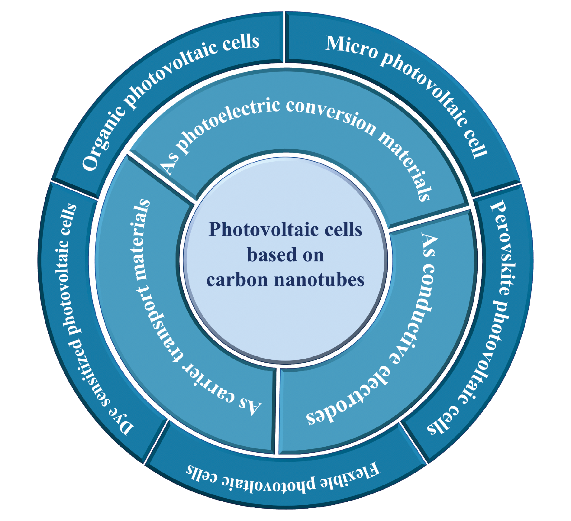
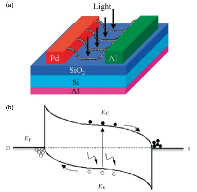
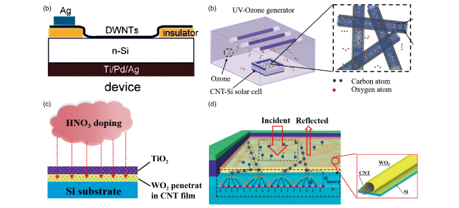
图4 (a)典型的碳纳米管/硅异质结太阳能电池结构[45];(b)气体掺杂结构示意图[47];(c)氧化钨掺杂的碳纳米管/硅异质结光伏电池结构[48];(d)碳纳米管/硅异质结光伏电池载流子传输途径示意图[48]

Fig. 4 (a) Typical CNT/silicon heterojunction solar cell structure[45]. (b) Schematic Diagram of gas doping Structure[47]. (c) Tungsten oxide doped CNT/silicon heterojunction photovoltaic cell structure[48]. (d) Schematic diagram of carrier transport paths of CNT/silicon heterojunction photovoltaic cells[48]

Element doping of CNT films can significantly improve the conversion efficiency of photovoltaic cells. For example, the CNT film is infiltrated in dilute nitric acid to achieve the acid doping effect. This method can significantly reduce the internal resistance of the CNT film and improve the carrier separation and transmission efficiency. Cao et al. Used a suspended catalyst CVD method to grow a network-like CNT film on a nickel foil[46]. The CNT film was subsequently transferred onto the silicon substrate by a transfer technique. And then that carbon nanotube film on the silicon substrate is soak in dilute nitric acid to obtain an acid-doped carbon nanotube/silicon heterojunction photovoltaic cell. The results show that the Jsc of untreated pristine carbon nanotube/silicon heterojunction photovoltaic cell is 47% for 27.4 mA/cm2,FF and 6.2% for PCE. After acid doping, the Jsc of carbon nanotube/silicon heterojunction photovoltaic cell is 72% for 36.3 mA/cm2,FF and 13.8% for PCE. Acid doping significantly improves the device photovoltaic performance. This is due to the fact that the series resistance of the CNT film is reduced after acid treatment, and the Rsh is reduced from 160 Ω/sq to 100 Ω/sq, resulting in a substantial increase in FF. In addition, the exposed silicon surface in the CNT film and the CNTs not in contact with the silicon wafer are covered by nitric acid after nitric acid treatment. Nitric acid can be used as an electrolyte to promote charge separation at the interface, and provide an additional charge transport path for the CNT network to improve the carrier separation efficiency. The disadvantage of this method is that the acid is volatile and corrosive to the silicon wafer, which degrades the photovoltaic performance of the device.
Cao et al. Directly exposed the carbon nanotube/silicon heterojunction photovoltaic cell to ozone to increase the hole concentration of the CNT film (as shown in Figure 4B)[47]. This method can enhance the built-in potential and Schottky barrier at the carbon nanotube/silicon heterojunction, and improve the performance of photovoltaic cell devices. Firstly, CNT films were prepared on nickel foil substrates by CVD technique. And then transfer to a silicon wafer by a wet method to form a CNT-Si photovoltaic cell; Finally, the integrated carbon nanotube/silicon photovoltaic heterojunction cell was exposed to ozone for 5 min. The Voc, FF and PCE were increased from 0. 498 V, 35.41% and 5. 29% to 0. 594 V, 78.13% and 12. 7%, respectively. Ozone treatment can increase the cell efficiency by more than 2 times. With the increase of exposure time, the transparency of the CNT film increased from 87. 84% to 92. 88%. Ozone acts as an electron acceptor and injects holes into CNTs during the charge transfer process due to its strong oxidizing property, which increases the work function of CNTs from 4. 27 eV to 4. 44 eV. This results in enhanced charge transfer across the CNT-Si interface and creates a larger built-in potential across the depletion width, which is directly responsible for the increase in Voc.
The introduction of a tungsten oxide (WO3) layer in carbon nanotube/silicon heterojunction photovoltaic cells has also been shown to be a viable option. Cao et al. Prepared CNT thin films on n-type silicon wafers by chemical vapor deposition[48]. Then, WO3 was deposited on the silicon wafer with porous CNT network by thermal evaporation deposition technology to prepare the WO3/CNT-Si photovoltaic cell (as shown in Figure 4C). The introduction of WO3 makes the Schottky barrier formed at the contact between WO3 and silicon. Because the work function of WO3 (5.2 eV) is much larger than that of CNT (4.19 eV),Lectron in that silicon wafer are extract to the WO3 side, holes are gathered on the surface of the silicon wafer to form an inversion lay, and finally a quasi-p-n junction is formed near the inside of the surface of the silicon wafer,The introduction of WO3 forms a cooperative mechanism (its carrier transmission pathway is shown in Figure 4D), CNT plays the role of charge collection and transmission, and WO3 also plays the role of anti-reflection layer to reduce the light absorption of photovoltaic cells, and forms a strong quasi-p-n junction on the silicon surface to achieve better charge separation.Due to the passivation effect of the WO3 on the silicon surface, the minority carrier lifetime is increased, the hole transmission is improved,The results show that the introduction of WO3 increases the VOC from 0. 43 V to 0.618 V,JSC, from 27.0 mA/cm2 to 29.97 mA/cm2,FF, from 54. 16% to 69. 26%.

3.3 Photovoltaic cell using carbon nanotubes as part of photosensitive material

CNTs can also be used in photovoltaic photosensitive materials as part of their components. On the one hand, CNTs can improve the conductivity efficiency of photosensitive materials and promote carrier migration, on the other hand, CNTs can improve the contact between photosensitive materials and carrier transport layer in photovoltaic cells, and promote carrier extraction by forming an interfacial polarization electric field. For example, Jin et al. Obtained carbon nanotubes (CNT:TiO2) modified by TiO2 particles by mixing CNTs with ethyl titanate in ethanol through hydrothermal treatment, and added them to the perovskite layer to obtain a perovskite photovoltaic cell with high stability (the structure is shown in Figure 5A)[49]. The Jsc of this photovoltaic cell are 24.85 mA/cm2,VOC of 1.2 V, FF of 76%, and PCE of 22.7%. Under the forward scan, the FF of the device is increased from 72% to 76%,Jsc and VOC by (FS),CNT:TiO2 doping (as shown in Fig. 5B). The interface polarization electric field generated by the contact interface between the CNT and the hole transport layer in the photosensitive layer promotes the carrier transfer, which makes the CNT:TiO2 modified perovskite photovoltaic cell have a higher current density. Compared with the unmodified perovskite photovoltaic cell, the integral current at the full wavelength is increased from 20.41 mA/cm2 to 23.74 mA/cm2,CNT:TiO2, and the carrier mobility of the doped perovskite layer is increased by 128%. The stability of the photovoltaic cell is improved due to the hydrophobicity of CNT:TiO2. After 744 H, the PCE of the perovskite photovoltaic cell doped with CNT:TiO2still maintains more than 91% of the initial efficiency, while the PCE of the control group doped with CNT:TiO2 is only 60%.
图5 (a)CNT:TiO2改性PSC结构示意图;(b)正向扫描(FS)和反向扫描(RS)下PSC的J-V曲线(w/o 无CNT:TiO2;w/ 有CNT:TiO2) [49]

Fig. 5 (a) Structural Diagram of CNT:TiO2 Modified PSC. (b) J-V curve of PSC under forward scan (FS) and reverse scan (RS) (w/o without CNT:TiO2; w/with CNT:TiO2) [49]

4 Carbon nanotube as conductive electrode

4.1 Application in organic photovoltaic cells

An organic photovoltaic cell (OSC) is usually composed of a single or double photoactive layer, an indium tin oxide (ITO) transparent positive electrode, and a metal negative electrode. ITO has been gradually banned because of its high brittleness, high cost of raw materials and high energy consumption in the manufacturing process. CNT thin films have good transparency, high conductivity, corrosion resistance and flexibility, and gradually replace the traditional ITO as a conductive electrode in organic polymer photovoltaic cells[50,51].
In recent years, CNT thin films have been widely studied as conductive electrodes for organic photovoltaic cells. Compared with the original SWCNT film electrode, improved methods including polymer composite, CNT film modification and noble metal doping have also been proved to improve the performance of photovoltaic cells[52]. For example, flexible photovoltaic cells based on polyaniline/CNT composite film electrodes[53]. Polyaniline/CNT composite film was prepared by interfacial polymerization self-assembly method, which had a transmittance of 89% at 550 nm and a sheet resistance of 295 Ω/sq. When it was used as a transparent electrode to replace ITO in flexible organic photovoltaic cells, the PCE reached 2. 27%.
Transparent conductive electrodes based on graphene composite carbon nanotubes have been shown to improve the performance of organic photovoltaic cells[54]. The dispersion prepared by sulfonated carbon nanotubes and graphene was applied to poly (3,4-ethylenedioxythiophene) -poly (styrenesulfonic acid) conductive polymer to prepare transparent conductive electrode. 85% transmittance in the visible range. The composite electrode was applied to organic polymer photovoltaic cells instead of ITO, and the PCE reached 5. 8%, which was higher than that of the photovoltaic device with ITO electrode. In similar reports, graphene and carbon nanotubes have been shown to have significant synergistic effects, improving the overall performance of photovoltaic cells[55].
The combination of CNT and noble metal materials has been proved to be a feasible solution to improve the performance of CNT film electrodes, such as CNT/silver nanowire (AgNW) multilayer electrodes for organic photovoltaic cells[56]. The mixed film of CNT and AgNW was firstly prepared on the polyethylene terephthalate (PET) substrate by the spray process, and the sheet resistance (Rsh) of the CNT/AgNW multilayer electrode would increase and the transmittance would decrease by increasing the number of cycles of spray. The electrode is matched on an organic photovoltaic cell with a P3HT: PCBM/PEDOT: PSS matrix. Under the illumination of 500 ~ 550 nm, the maximum transmittance is 50 Ω/sq, the fill factor is 48. 05%, and the maximum PCE is 2. 21%, which is 0. 78% higher than that using only AgNW electrode. With the increase of spraying cycles, the transmittance decreases, resulting in a decrease of PCE to 1.12%.

4.2 Application in perovskite photovoltaic cells.

Perovskite photovoltaic cell (PSC) refers to a photovoltaic cell with perovskite structure materials as the light absorption layer, which usually has a five-layer structure, including a cathode layer, an electron transport layer, a light absorption layer, a hole transport layer and an anode layer. The cathode layer and the anode layer serve as the conductive electrodes of the photovoltaic cell, which are usually composed of ITO and FTO (fluorine-doped tin oxide). In recent years, CNT films have been used as conductive electrodes in perovskite photovoltaic cells due to their flexibility, transparency, high conductivity and suitable work function[57,58]. The CNT conductive electrode used in perovskite photovoltaic cells in the early stage was composed of translucent carbon nanotube film prepared by CVD, which was covered on the surface of perovskite active layer by transfer technology to realize electrode construction. The PCE of this photovoltaic cell reached 6.87%[59]. After development in recent years, the PCE value of PSC assembled with SWCNT as back electrode is 9. 9%, which is significantly higher than that of PSC assembled with Au back electrode (3. 8%) under the same conditions[60].
Doping or compounding of CNT film electrode has been proved to be an effective method to improve the overall performance of PSC, and CNT can play a good synergistic role, such as PSC back electrode obtained by iodine doping of CNT film[61]. Carbon nanotube arrays with a length of 300 mm were prepared by low pressure chemical vapor deposition (LP-CVD) using iron as catalyst and acetylene as precursor, and then cross-stacked CNT films were obtained by repeatedly extracting and stacking from the carbon nanotube arrays. The CNT film was placed in iodine vapor to achieve doping. Iodine-doped CNT films improve the electrical conductivity of CNTs and the particle size and crystallinity of perovskite in carbon nanotube films. The short-circuit current density and fill factor of PSC are significantly improved due to the reduction of carrier recombination of carbon nanotubes by iodine element. The PCE of PSC with cross-stacked carbon nanotube film electrode can reach 8. 65%, and the PCE of PSC with iodine doping can reach 10. 54%. In another study, the composite of carbon nanotubes and graphene was proved to have a good synergistic effect. The composite was formed by the hydrothermal reaction of the mixed solvent of carbon nanotubes and graphene and the titanium oxide precursor, and the transparent conductive electrode layer was obtained after spin coating[62]. The results show that the PCE of the PSC with CNT and graphene composite electrode is 0.9 V for 13.97%,Jsc and 24.8 mA/cm2,Voc, and the FF is 62.5%, which is 43.4% higher than that of the pure TiO2 conductive electrode in terms of Jsc.In the photoanode of PSC, the charge collection at the perovskite interface can be significantly improved, and the work function of graphene and CNT is between TiO2 and FTO, which can significantly reduce the TiO2/FTO interface energy barrier to promote electron collection. On the one hand, CNT and graphene in the composite help to improve the current density, on the other hand, when the content of CNT and graphene is higher than 0. 5 wt%, the transparency of the electrode layer will be significantly reduced, and the agglomeration of carbon materials will be sharply increased, which will reduce the conversion efficiency of PSC.

4.3 Application in dye-sensitized photovoltaic cell

DSSC consists of three parts: platinum coating as counter electrode (CE), titanium oxide (TiO2) nanocrystals after dye sensitization, and liquid iodide/triiodide as electrolyte. The working principle of the photovoltaic cell is as follows: dye molecules adsorbed on the surface of the TiO2 generate excited electrons by transition under illumination, and the electrons are injected into the conduction band of the TiO2 and enriched to the photocathode,The dye molecules that have lost electrons become oxidized and undergo an oxidation reaction in the electrolyte, and the electron donors in the electrolyte undergo a reduction reaction at the anode to obtain electrons, and finally a voltage is formed across the electrode. At present, the mainstream DSSC uses platinum electrodes, but the scarcity of platinum metal limits its large-scale application, and the search for alternatives to platinum metal is the current research focus in the field of DSSC.
CNTs serve as a potential additive material to improve the electrode performance due to their excellent electrical conductivity. For example, Cheruku et al. Prepared DSSCs using polypyrrole and sodium dodecyl sulfate composite carbon nanotubes (PPy + SDS + CNT) as electrodes[63]. A PPy + SDS + CNT film was deposited on fluorine-doped tin oxide (FTO) glass by electrochemical polymerization, and was used as an electrode layer material in a DSSC (structure shown in Figure 6a). The surface morphology of the film after adding CNTs (Figure 6B) showed that CNTs were uniformly spread in it, forming a good conductive network. The Jsc of the photovoltaic cell were 15.47 mA/cm2,VOC of 0.67 V, FF of 58.69%, and PCE of 6.15%. Compared with the PPy + SDS electrode without CNTs, the PPy + SDS + CNT electrode has a higher short-circuit current (as shown in Figure 6C), which is related to the penetration of CNTs throughout the layer. The addition of CNT increased the PCE of DSSCs from 5. 84% to 6. 15%. The photoelectric conversion efficiency (IPCE) of the photovoltaic cell is also improved at the full wavelength (Figure 6d). In another study, carbon nanotubes and Ni2P nanocrystals formed a composite (CNT-Ni2P) as a cathode layer material also showed similar performance to Pt-FTO[64]. Compared with the single counter electrode of CNT and Ni2P, the charge transfer resistance and diffusion impedance of the CNT-Ni2P counter electrode are lower, which are close to those of the FTO counter electrode, the photocurrent reaches 12.9 mA/cm2, and the energy conversion efficiency reaches 5. 6%, which is close to the energy conversion efficiency of the Pt-FTO DSSC (5. 9%).
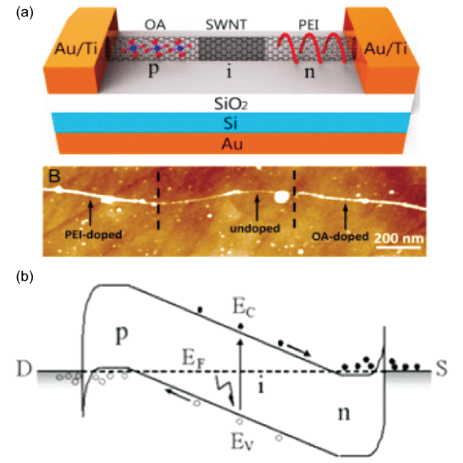
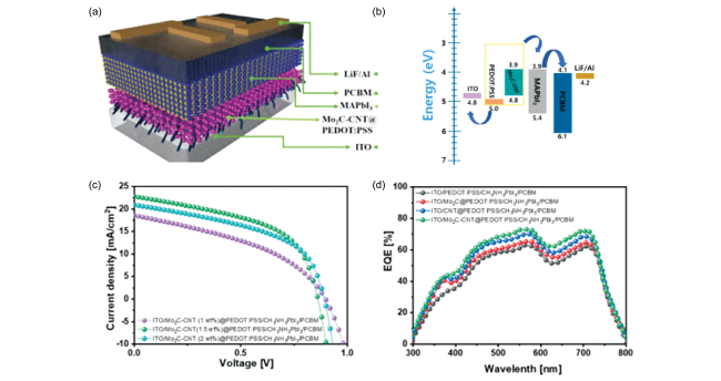
图6 (a)碳纳米管透明导电电极的染料敏化光伏电池结构示意图;(b)电极层表面形貌图;(c)不同电极下DSSC的J-V曲线;(d)不同对电极下DSSC的IPCE曲线[63]

Fig. 6 (a) Structure diagram of DSSC cell with CNT transparent conductive electrode. (b) Surface topography of electrode layer. (c) J-V curve of DSSC with different electrodes. (d) IPCE curve of DSSC under different pair electrodes[63]

It is feasible to use multi-walled carbon nanotubes (MWCNTs) as the transparent conductive electrode of DSSC. For example, the counter electrode of DSSC prepared by multi-walled carbon nanotubes (MWCNTs) grown on nickel substrate by ethanol flame method shows good conductivity and photoelectric conversion efficiency[65]. Compared with the DSSC based on Pt/FTO-CE (short-circuit current density 13.8 mA/cm2,PCE of 6.72%), the DSSC based on MWCNT electrode shows a larger short-circuit current density (14.7 mA/cm2) and a higher photoelectric conversion efficiency (PCE of 7.43%).

4.4 Application in flexible photovoltaic cell

Flexible photovoltaic cells have the characteristics of lightness, flexibility and compatibility with roll-to-roll preparation process, which is an important research direction of new photovoltaic cells. Flexible photovoltaic cells require that all functional layers must be made of flexible materials, and the materials used for electrode layers are more stringent. Because the flexible electrode is often used as the substrate of the active layer, the interaction between the flexible electrode and the active layer affects the interface and micro-morphology of each functional layer, and affects the overall performance of the flexible photovoltaic cell[25,53]. CNT is an ideal material for the construction of flexible electrodes due to its excellent conductivity, mechanical properties and ultra-high specific surface area, and has been used as a flexible electrode in PSC and OSC.
Due to the excellent mechanical properties of CNT, the method of mixing it as a conductive network with polymers to form composite electrodes can improve the mechanical properties of flexible electrodes. Yoon et al. Used a SWCNT film doped with MoO3 to embed into polyimide (PI) to obtain a SWNT-PI flexible electrode, and applied it to PSC to obtain a foldable flexible perovskite photovoltaic cell. First, a high-purity and long-bundle SWCNT film was synthesized by CVD method, and the SWCNT film was transferred to a quartz substrate deposited with MoO3 by a continuous transfer process.Then the PI precursor solution was spin-coated on the SWCNT/quartz substrate, and after curing treatment, the SWNT-PI flexible electrode was obtained, which was applied in the flexible PSC with SWNT-PI/MoOx/ polytriarylamine (PTAA)/Perovskite/C60/2,9- dimethyl-4,7-diphenyl-1,10-phenanthroline (BCP)/Cu structure, and the Jsc of the photovoltaic cell was 19.0 mA/cm2,VOC of 1. 05 V, FF of 76. 6%, and PCE of 15. 2%[66]. Its advantage is high mechanical stability, which can withstand more than 10,000 cycles of folding at a folding radius of 0.5 mm. However, the ITO electrode PSC under the same process showed severe performance degradation after 1000 cycles of folding with 4 mm bending. This is because the SWNT-PI flexible electrode avoids the interfacial contact between the SWNT and the TiO2 layer during the folding process. Compared with no PI, SWNT-PI can significantly reduce the thickness of PTAA layer to reduce the device resistance. In addition, the SWNT-PI flexible electrode is only 7 μm thick, which is one of the reasons for the excellent mechanical resilience of photovoltaic cells.
The p-doping of CNT film with MoO3 can improve the electrical conductivity of CNT film flexible electrode, and the MoO3 on CNTs can be reduced to MnOx to induce stable p-doping of CNTs, which increases the hole carrier concentration and reduces the Fermi level of CNTs. Matsuo et al. Used the MoO3 doped CNT film as the flexible conductive transparent electrode of organic photovoltaic cells, and the work function of the CNT film was increased from 4.86 eV to 5.4 eV by MoO3 doping. In addition, the transmittance of the CNT film was improved in all bands after doping[67].

5 Carbon nanotubes as carrier transport materials

In order to improve the conversion efficiency and structural stability of photovoltaic cells, two transport layers for charge collection and extraction are usually added to the photovoltaic cell structure. The two transport layers, an electron transport layer (ETL) and a hole transport layer (HTL), respectively, are sandwiched between the photosensitive layer and the conductive electrode. ETL and HTL play a decisive role in the conversion efficiency and stability of photovoltaic cells. Materials such as Polyfluorene derivative (PFN), perylene diimide (PDI), polyethyleneimine (PEI), titanium oxide, and zinc oxide are usually used in ETL to extract electrons from the active layer and avoid carrier recombination in the active layer[68~72]. HTL usually uses copper oxide, iron oxide, nickel oxide and cuprous thiocyanate to extract holes in the active layer and avoid carrier recombination in the active layer[73,74]. The application of these materials as HTL is limited by their poor conductivity and low carrier mobility. Therefore, the selection of materials with high conductivity, appropriate work function, high transparency and easy processing as the carrier transport layer of photovoltaic cells has become a hot research topic. CNTs have been widely studied as a HTL to adjust the carrier transfer and collection characteristics.
Kang et al. Mixed the Mo2C-CNT hybrid nanostructure with PEDOT: PSS as perovskite photovoltaic cell HTL by preparation[75]. Firstly, Mo2C and CNT were dispersed in ethanol by ultrasonic, and stable hybrid nanomaterials were obtained after centrifugation and annealing. Then, Mo2C-CNT hybrid nanostructure mixed with PEDOT: PSS was spin-coated on the ITO surface to obtain HTL after further annealing process; The final application of PSC in ITO/HTL/CH3NH3PbI3/PCBM/LiF/Alstructure (its structure is shown in Figure 7 a), the Voc of this photovoltaic cell is 61% for 0.862 V,Jsc and 22.78 mA/cm2,FF.The optical conversion efficiency PCE is 11.98%, and the device Rs is reduced from 176.31Ω·cm2 to 159.22Ω·cm2 after HTL doping into the Mo2C-CNT hybrid nanostructure. Since the introduction of Mo2C/CNT enhances the HTL internal electric field and makes the band positions correlated with each other (as shown in Figure 7 B), the rapid separation and transport of charges are promoted. The performance of the device can be controlled by adjusting the content of CNTs (Fig. 7c), in which the PCE of the device is the largest when the concentration of CNTs is 1.5 wt%. The external quantum efficiency (EQE) spectrum of the HTL in the wavelength range of 300 ~ 800 nm (Fig. 7d) shows that the highest EQE is obtained by doping Mo2C-CNT at the same time, which proves the synergistic behavior of the two materials.
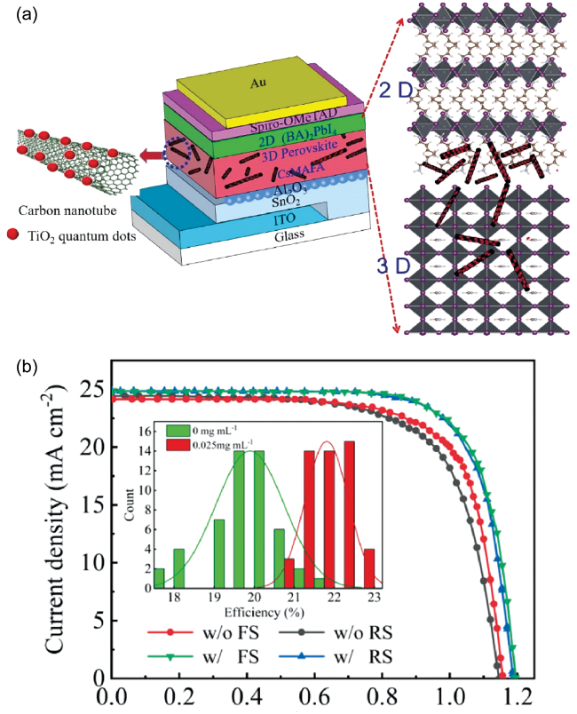
图7 (a)使用Mo2C-CNTs@PEDOT:PSS作为 HTL的光伏电池结构;(b)使用Mo2C-CNTs@PEDOT:PSS作为 HTL的钙钛矿光伏电池的能级图;(c)碳纳米管质量分数分别为1%(紫),1.5%(绿),2.0%(蓝)PSC的J-V曲线;(d)不同组分的HTL下(HTL中未加入Mo2C-CNTs(黑)、只加入Mo2C(红)、只加入CNTs(蓝)、加入Mo2C-CNTs(绿)的),PSC的外部量子效率(EQE)谱[75]

Fig. 7 (a) PV cell structure using Mo2C-CNTs@PEDOT:PSS as HTL. (b) Energy level diagram of perovskite photovoltaic cells using Mo2C-CNTs@PEDOT:PSS as HTL. (c) J-V curve of PSC with 1% (purple), 1.5% (green) and 2.0% (blue) carbon nanotubes. (d) External quantum efficiency (EQE) spectrum of PSC under HTL with different components (no Mo2C-CNTs (black), only Mo2C (red), only CNTs (blue), and Mo2C-CNTs (green) added in HTL) [75]

Markose et al. Mixed the CNT film with PEDOT: PSS and used it as the HTL of organosilicon hybrid heterojunction photovoltaic cells[76]. Compared with the PEDOT: PSS/Si photovoltaic cell, the Voc of the PEDOT: PSS/Si photovoltaic cell is 502 mV,Jsc to be 29.5 mA/cm2,FF 41.5%, the light conversion efficiency PCE is 6.02%,The Voc of this hybrid heterojunction photovoltaic cell is 588.6 mV,Jsc to 25.3 mA/cm2,FF 60.79% with a photoconversion efficiency PCE of 9.05%. On the one hand, the introduction of CNT forms a strong inversion layer at the interface, which inhibits the carrier recombination at the heterojunction and improves the carrier extraction rate. On the other hand, the addition of CNT improves the conductivity of the composite film and enhances the lateral transport of electrons to the electrode.

6 Conclusion and outlook

In this paper, the different structural characteristics, preparation methods and optimization strategies of carbon nanotubes used as photoelectric conversion materials, conductive electrodes and carrier transport layers in photovoltaic cells in recent years are reviewed. Carbon nanotubes (CNTs) are considered to be ideal candidate materials for photovoltaic cells due to their excellent photoelectric properties, and their good chemical stability, flexible processability and abundant carbon reserves are conducive to the industrial production and application of CNT-based photovoltaic cells. The development status and future challenges of carbon nanotubes in the field of photovoltaic cells are summarized here.
(1) When carbon nanotubes are used as photoelectric conversion materials, they are mainly used as some components of photosensitive layers of micro-photoelectric devices, carbon nanotube/silicon heterojunction photovoltaic cells and other photovoltaic cells. In this kind of photovoltaic cell, a strong built-in electric field is formed inside the carbon nanotube or between the carbon nanotube and other materials to promote the separation and collection of photogenerated carriers and realize the photovoltaic effect. Device performance can be improved by doping techniques and material recombination such as acid treatment, gas adsorption, and metal oxide recombination. At present, the doping technology of carbon nanotubes has been widely studied, but the stability of these doping technologies is poor. It is of great significance to obtain highly stable carbon nanotube doping technology for its application as a photoelectric conversion material.
(2) When carbon nanotubes are used as conductive electrodes, they are mainly used in new generation photovoltaic cells, including dye-sensitized and perovskite organic photovoltaic cells. This type of photovoltaic cell mainly relies on the excellent conductivity and mechanical stability of carbon nanotubes to achieve efficient carrier collection. Especially in terms of mechanical properties, carbon nanotubes can well replace ITO as electrode materials for flexible photovoltaic cells. At present, carbon nanotubes are widely used to replace expensive Pt, Au or ITO as conductive electrodes. The improvement methods include carbon nanotube composite, surface modification and metal or metal oxide doping, which improve the conversion efficiency of photovoltaic cells. However, there are still many challenges to be overcome for the industrial application of such photovoltaic cells. For example, the conductivity and optical transparency of carbon nanotubes are lower than those of ITO electrodes, and new carbon nanotube preparation technologies need to be developed to improve such properties.
(3) When carbon nanotubes are used as a carrier transport layer, their appropriate work function contributes to the effective extraction of holes, and their good conductivity contributes to the efficient transport of holes. The problem with this type of photovoltaic cell is the low stability, including thermal stability and humidity stability. Although the addition of carbon nanotubes has a promoting effect, better modification technologies are still needed to improve their stability, among which the use of carbon nanotubes composite is still a feasible solution, including the formation of efficient synergistic systems with graphene and the formation of composite materials with polymers.
Although carbon nanotubes have been widely studied in the field of photovoltaic cells, these studies are still in the laboratory stage, and how to widely apply carbon nanotube-based photovoltaic cells to social production is still a challenging problem. Because the purification and dispersion of carbon nanotubes is still a big problem, the current carbon nanotubes with single and uniform dispersion are not only expensive but also have many defects. The optical and electrical properties of carbon nanotube films are far below the ideal value due to the inevitable incorporation of other types of carbon nanotubes into the films. Finding a simple, environmentally friendly and low-cost preparation process for carbon nanotubes, as well as an improved method to minimize the agglomeration and structural defects of carbon nanotubes, is still a necessary way to improve the development of carbon nanotube-based photovoltaic cells in the future, and on this basis, compounding and doping with different materials is still a good way to improve the performance of photovoltaic cells.
[1]
Jurasz J, Canales F A, Kies A, Guezgouz M, Beluco A. Sol. Energy, 2020, 195: 703.

[2]
Hayat M B, Ali D, Monyake K C, Alagha L, Ahmed N. Int. J. Energy Res., 2019, 43(3): 1049.

[3]
Wang J Q, Xie Z M, Yeow J T W. ECS J. Solid State Sci. Technol., 2020, 9(10): 105004.

[4]
Fukuda K, Yu K, Someya T. Adv. Energy Mater., 2020, 10(25): 2000765.

[5]
Ortiz-Cervantes C, Carmona-Monroy P, Solis-Ibarra D. ChemSusChem, 2019, 12(8): 1560.

[6]
Yun S N, Qin Y, Uhl A R, Vlachopoulos N, Yin M, Li D D, Han X G, Hagfeldt A. Energy Environ. Sci., 2018, 11(3): 476.

[7]
Qiu L B, Deng J, Lu X, Yang Z B, Peng H S. Angew. Chem. Int. Ed., 2014, 53(39): 10425.

[8]
Kaltenbrunner M, Adam G, Daniel Głowacki E, Drack M, Schwödiauer R, Leonat L, Apaydin D H, Groiss H, Scharber M C, White M S, Sariciftci N S, Bauer S. Nat. Mater., 2015, 14(10): 1032.

[9]
Zhang Y K, Wu Z W, Li P, Ono L K, Qi Y B, Zhou J X, Shen H, Surya C, Zheng Z J. Adv. Energy Mater., 2018, 8(1): 1701569.

[10]
Gu S, Lin R X, Han Q L, Gao Y, Tan H R, Zhu J. Adv. Mater., 2020: 1907392.

[11]
Zhao C C, Wang J X, Zhao X Y, Du Z L, Yang R Q, Tang J G. Nanoscale, 2021, 13(4): 2181.

[12]
Urbani M, Ragoussi M E, Nazeeruddin M K, Torres T. Coord. Chem. Rev., 2019, 381: 1.

[13]
Jalalvand A R, Ghobadi S, Akbari V, Goicoechea H C, Faramarzi E, Mahmoudi M. Sens. Bio Sens. Res., 2019, 25: 100297.

[14]
Zhao X, Park N G. Photonics, 2015, 2(4): 1139.

[15]
Li W J, Zheng J H, Hu B, Fu H C, Hu M W, Veyssal A, Zhao Y Z, He J H, Leo Liu T, Ho-Baillie A, Jin S. Nat. Mater., 2020, 19(12): 1326.

[16]
Abate A, Correa-Baena J P, Saliba M, Su’ait M S, Bella F. Chem. Eur. J., 2018, 24(13): 3083.

[17]
Tumbul A, Aslan F, Gökta塂 A, Mutlu I H. J. Alloys Compd., 2019, 781: 280.

[18]
Fagiolari L, Bella F. Energy Environ. Sci., 2019, 12(12): 3437.

[19]
Li D D, Lai W Y, Zhang Y Z, Huang W. Adv. Mater., 2018, 30(10): 1704738.

[20]
Lee S K, Rana K, Ahn J H. J. Phys. Chem. Lett., 2013, 4(5): 831.

[21]
De Volder M F L, Tawfick S H, Baughman R H, Hart A J. Science, 2013, 339(6119): 535.

[22]
Ma P C, Siddiqui N A, Marom G, Kim J K. Compos. A Appl. Sci. Manuf., 2010, 41(10): 1345.

[23]
Wen L, Li F, Cheng H M. Adv. Mater., 2016, 28(22): 4306.

[24]
Jung S, Lee J, Seo J, Kim U, Choi Y, Park H. Nano Lett., 2018, 18(2): 1337.

[25]
Fu X M, Xu L M, Li J X, Sun X M, Peng H S. Carbon, 2018, 139: 1063.

[26]
Tune D D, Flavel B S. Adv. Energy Mater., 2018, 8(15): 1703241.

[27]
Luo Q, Wu R G, Ma L T, Wang C J, Liu H, Lin H, Wang N, Chen Y, Guo Z H. Adv. Funct. Mater., 2021, 31(6): 2004765.

[28]
Batmunkh M, Biggs M J, Shapter J G. Small, 2015, 11(25): 2963.

[29]
Yu L P, Shearer C, Shapter J. Chem. Rev., 2016, 116(22): 13413.

[30]
Mann D, Javey A, Kong J, Wang Q, Dai H J. Nano Lett., 2003, 3(11): 1541.

[31]
Chen G H, Futaba D N, Sakurai S, Yumura M, Hata K J. Carbon, 2014, 67: 318.

[32]
in het Panhuis M. J. Mater. Chem., 2006, 16(36): 3598.

[33]
Frank S, Poncharal P, Wang Z L, de Heer W A. Science, 1998, 280(5370): 1744.

[34]
Guo J, Lundstrom M, Datta S. Appl. Phys. Lett., 2002, 80(17): 3192.

[35]
Liang W J, Bockrath M, Bozovic D, Hafner J H, Tinkham M, Park H. Nature, 2001, 411(6838): 665.

[36]
Ebbesen T W, Lezec H J, Hiura H, Bennett J W, Ghaemi H F, Thio T. Nature, 1996, 382(6586): 54.

[37]
Odom T W, Huang J L, Kim P, Lieber C M. Nature, 1998, 391(6662): 62.

[38]
Blackburn J L, Barnes T M, Beard M C, Kim Y H, Tenent R C, McDonald T J, To B, Coutts T J, Heben M J. ACS Nano, 2008, 2(6): 1266.

[39]
Huang Q J, Zhu Y. Adv. Mater. Technol., 2019, 4(5): 1800546.

[40]
Ferguson V, Silva S R P, Zhang W. Energy Environ. Mater., 2019, 2(2): 107.

[41]
Wang C Y, Xia K L, Wang H M, Liang X P, Yin Z, Zhang Y Y. Adv. Mater., 2019, 31(9): 1801072.

[42]
Cinke M, Li J, Chen B, Cassell A, Delzeit L, Han J, Meyyappan M. Chem. Phys. Lett., 2002, 365(1/2): 69.

[43]
Chen C X, Lu Y, Kong E S, Zhang Y F, Lee S T. Small, 2008, 4(9): 1313.

[44]
Chen C X, Song C J, Yang J R, Chen D Q, Zhu W H, Liao C H, Dong X S, Liu X D, Wei L M, Hu N T, He R, Zhang Y F. Nano Energy, 2017, 32: 280.

[45]
Wei J Q, Jia Y, Shu Q K, Gu Z Y, Wang K L, Zhuang D M, Zhang G, Wang Z C, Luo J B, Cao A Y, Wu D H. Nano Lett., 2007, 7(8): 2317.

[46]
Jia Y, Cao A Y, Bai X, Li Z, Zhang L H, Guo N, Wei J Q, Wang K L, Zhu H W, Wu D H, Ajayan P M. Nano Lett., 2011, 11(5): 1901.

[47]
Zhao X W, Wu H S, Yang L S, Wu Y Z, Sun Y P, Shang Y Y, Cao A Y. Carbon, 2019, 147: 164.

[48]
Zhao X W, Xu W J, Wu Y Z, Wu H S, Xia Z Y, Xu H Y, Shang Y Y, Wei J Q, Cao A Y. Nano Res., 2022, 15(3): 2497.

[49]
Jin M Q, Li H L, Lou Q, Du Q, Huang Q S, Shen Z T, Li F M, Chen C. EcoMat, 2022, 4(2): e12166.

[50]
Muchuweni E, Mombeshora E T, Martincigh B S, Nyamori V O. Front. Chem., 2022, 9: 733552.

[51]
Zhu Y Y, Shu L, Fan Z Y. Chem. Res. Chin. Univ., 2020, 36(3): 366.

[52]
Rowell M W, Topinka M A, McGehee M D, Prall H J, Dennler G, Sariciftci N S, Hu L B, Gruner G. Appl. Phys. Lett., 2006, 88(23): 233506.

[53]
Salvatierra R V, Cava C E, Roman L S, Zarbin A J G. Adv. Funct. Mater., 2013, 23(12): 1490.

[54]
Ji T, Tan L C, Bai J X, Hu X T, Xiao S Q, Chen Y W. Carbon, 2016, 98: 15.

[55]
Zhang Z X, Lv R T, Jia Y, Gan X, Zhu H W, Kang F Y. Appl. Sci., 2018, 8(2): 152.

[56]
Yang M K, Lee J K. Electron. Mater. Lett., 2020, 16(6): 573.

[57]
Lu L Y, Xu T, Chen W, Lee J M, Luo Z Q, Jung I H, Park H I, Kim S O, Yu L P. Nano Lett., 2013, 13(6): 2365.

[58]
Fan Q X, Zhang Q, Zhou W B, Xia X G, Yang F, Zhang N, Xiao S Q, Li K W, Gu X G, Xiao Z J, Chen H L, Wang Y C, Liu H P, Zhou W Y, Xie S S. Nano Energy, 2017, 33: 436.

[59]
Li Z, Kulkarni S A, Boix P P, Shi E Z, Cao A Y, Fu K W, Batabyal S K, Zhang J, Xiong Q H, Wong L H, Mathews N, Mhaisalkar S G. ACS Nano, 2014, 8(7): 6797.

[60]
Aitola K, Sveinbjörnsson K, Correa-Baena J P, Kaskela A, Abate A, Tian Y, Johansson E M J, Grätzel M, Kauppinen E I, Hagfeldt A, Boschloo G. Energy Environ. Sci., 2016, 9(2): 461.

[61]
Luo Q, Ma H, Zhang Y, Yin X W, Yao Z B, Wang N, Li J B, Fan S S, Jiang K L, Lin H. J. Mater. Chem. A, 2016, 4(15): 5569.

[62]
Amini A, Abdizadeh H, Golobostanfard M R. ACS Appl. Energy Mater., 2020, 3(7): 6195.

[63]
Lee J H, Jang Y J, Kim D W, Cheruku R, Thogiti S, Ahn K S, Kim J H. Chem. Pap., 2019, 73(11): 2749.

[64]
Dou Y Y, Yan N F, Li G R, Gao X P. J. Appl. Electrochem., 2012, 18(4): 301.

[65]
Zheng L, Bao C, Lei S J, Wang J L, Li F X, Sun P P, Huang N, Fang L, Sun X H. Carbon, 2018, 133: 423.

[66]
Yoon J, Kim U, Yoo Y, Byeon J, Lee S K, Nam J S, Kim K, Zhang Q, Kauppinen E I, Maruyama S, Lee P, Jeon I. Adv. Sci., 2021, 8(7): 2004092.

[67]
Jeon I, Cui K H, Chiba T, Anisimov A, Nasibulin A G, Kauppinen E I, Maruyama S, Matsuo Y. J. Am. Chem. Soc., 2015, 137(25): 7982.

[68]
Yan Y, Li W, Cai J L, Chen M X, Mao Y C, Chen X L, Gurney R S, Liu D, Huang F, Wang T. Mater. Chem. Front., 2018, 2(10): 1859.

[69]
Yan W B, He Z X, Jiang J J, Lu D, Gong Y C, Yang W S, Xia R D, Huang W, Xin H. J. Mater. Chem. C, 2020, 8(42): 14773.

[70]
Li M Y, Zha W S, Han Y F, Liu B W, Luo Q, Ma C Q. Org. Electron., 2021, 96: 106257.

[71]
Chaudhary J, Gupta S K, Verma A S, Negi C M S. J. Mater. Sci., 2020, 55(10): 4345.

[72]
Bai S, Jin Y Z, Liang X Y, Ye Z Z, Wu Z W, Sun B Q, Ma Z F, Tang Z, Wang J P, Würfel U, Gao F, Zhang F L. Adv. Energy Mater., 2015, 5(5): 1401606.

[73]
Yu Z K, Fu W F, Liu W Q, Zhang Z Q, Liu Y J, Yan J L, Ye T, Yang W T, Li H Y, Chen H Z. Chin. Chemical Lett., 2017, 28(1): 13.

[74]
Hu W, Liu T, Yin X W, Liu H, Zhao X Y, Luo S P, Guo Y, Yao Z B, Wang J S, Wang N, Lin H, Guo Z H. J. Mater. Chem. A, 2017, 5(4): 1434.

[75]
Hussain S, Liu H L, Vikraman D, Hussain M, Jaffery S H A, Ali A, Kim H S, Kang J, Jung J. J. Alloys Compd., 2021, 885: 161039.

[76]
Markose K K, Jasna M, Subha P P, Antony A, Jayaraj M K. Sol. Energy, 2020, 211: 158.

Outlines

/