
Preparation, Application and Prospect of RIfS Interference Substrates
Received date: 2023-04-10
Revised date: 2023-09-10
Online published: 2023-11-30
Supported by
Open Research Fund of State Key Laboratory ofDigital Medical Engineering(2023-K13)
Shuangchuang Ph.D award of Jiangsu province(JSSCBS20211301)
Doctoral research project of Jiangsu Ocean University(KQ21002)
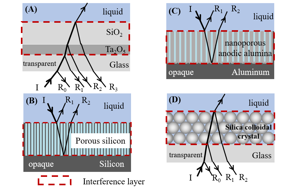
Reflectometric interference spectroscopy (RIfS) is a label-free detection technique by measuring the optical thickness of thin films which is based on white light interference. Interference effective substrates, as the sensor unit of the RIfS system, the construction of which is the core part of RIfS technology and the key to determining the performance of the RIfS system. Currently used interference substrates are generally divided into two categories: one is the planar solid substrates represented by inorganic oxides or polymer films, and the other is the porous substrates represented by porous silicon (pSi), nanoporous anodic alumina (NAA) and silica colloidal crystals (SCC). The preparation of planar solid substrate is simple and the signal is stable, but the detection sensitivity is usually low. In comparison with planar solid substrates, a porous substrate can provide a three-dimensional structure with a large specific surface area which will result in increased ligand immobilization density and capture of analyte. Therefore, the detection sensitivity is improved and there is more room for adjustment, which is very suitable for the development of a biochemical sensing platform. From pSi to NAA to SCC, the preparation controllability and sensing performance of porous substrates are continuously improved, which is considered a promising development direction of RIfS interference substrate. Here, the research status of RIfS interference substrates has been summarized and discussed, the common preparation methods of substrates are described, their representative applications in biosensing are summarized, the advantages and disadvantages of different substrates are discussed, and the future development directions of RIfS interference substrates has also been outlined.
1 Introduction
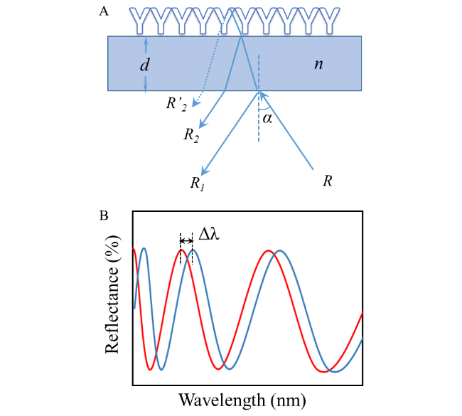
2 Measurement principles of reflectometric interference spectroscopy
3 Interference substrate
3.1 Planar solid substrate
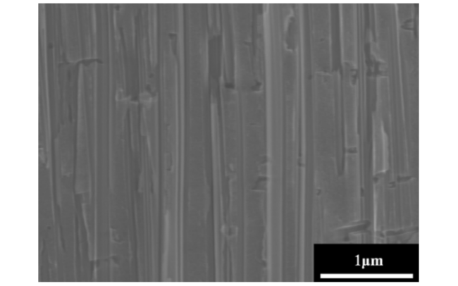
3.2 Porous silicon substrate
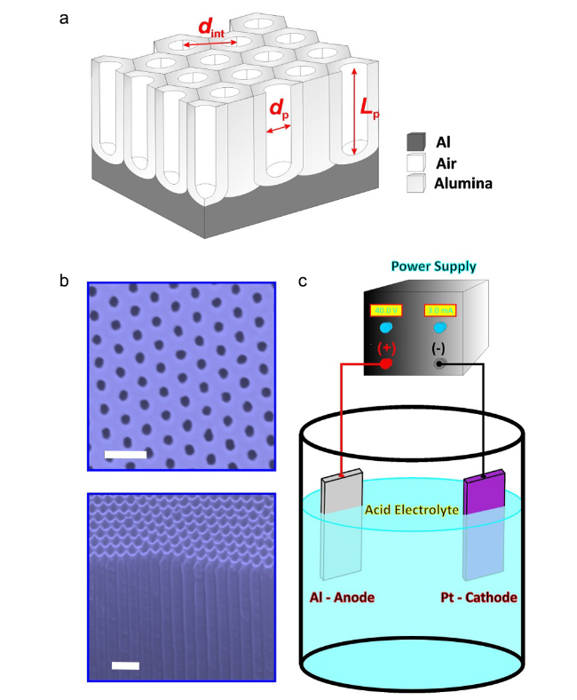
3.3 Nanoporous anodic alumina substrate
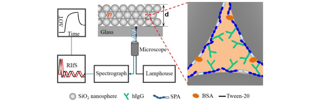
3.4 Silica colloidal crystals substrate
4 Conclusion and outlook
Qianqian Su , Yu Sun , Wenwen Zhang , Zhengde Peng , Weiping Qian . Preparation, Application and Prospect of RIfS Interference Substrates[J]. Progress in Chemistry, 2023 , 35(12) : 1793 -1806 . DOI: 10.7536/PC230410
| Analyte under analysis | Probe molecule | Detection range | Limit of detection | Response time(min) |
|---|---|---|---|---|
| DNA (15 mer) | ssDNA | 1~10 nmol/L | 1 nmol/L | 20 |
| Subtilisin | Gelatin | 0.37~370 nmol/L | 370 pmol/L | 20 |
| Sortase-A | Fluorogenic peptide | 4.6~46 000 pmol/L | 0.08 pmol/L | 30 |
| Sheep IgG | Protein A | 10~500 μg/mL | 0.6 μg/mL | 90 |
| Bacteria (E. coli) | Peptide | 103~105 cells/mL | 103 cells/mL | 60 |
| Streptavidin | Biotin | 0.5~5 μmol/L | 0.5 μmol/L | 20 |
| Vancomycin | Peptide | 0.005~0.1 mg/mL | 5 μg/mL | 20 |
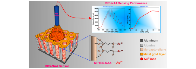
图3 (a) 纳米孔阳极氧化铝基底的结构示意图;(b) 纳米孔阳极氧化铝基底的正面及侧面SEM图(图中标尺分别为400和250 nm);(c) 纳米孔阳极氧化铝基底的制备装置示意图[65]Fig. 3 (a) Illustrative scheme describing the most representative geometric features of nanoporous anodic alumina (NAA); (b) top and cross-section scanning electron microscopy (SEM) images of NAA (scale bars = 400 and 250 nm, respectively); (c) illustration describing a basic electrochemical anodisation cell used to produce NAA[65] |
| Method | Remarks |
|---|---|
| Drop casting (Sedimentation) | Simple but slow process. Patches of colloidal crystals formed. Difficult to control exact conditions |
| Centrifugation | Simple and fast process. Generally big bulky colloidal crystals formed. |
| Spin-coating | Simple and fast process. Monolayer formation possible. Patches of small coating area of monolayers. |
| Dip-coating | Can control thickness of layers by the speed of withdrawal. Gradient in layer thickness. |
| Shear ordering | Requires very good control of process parameters. Slow process. Makes thin films. |
| Langmuir-Blodgett | Monolayer compressed on water surface by mobile arms. Short range order of closed packed regions within the monolayer. Monolayer transfer onto substrate can be repeated to deposit multilayers exactly as desired. Takes time for preparation of equipment and spreading of particles. |
| Direct assembly on water surface | Simple and fast process. Good two-dimensional closed pack array on water surface. One monolayer at a time can be transferred. Can be repeated to deposit multilayers exactly as desired. |
| Magnetic self-assembly | Requires highly-charged monodisperse magnetic colloidal particles. Self-assembly occurs inside liquid medium. Can be controlled by external magnetic field. |
| Vertical deposition | Requires very good control of evaporation conditions (i.e., temperature and humidity) for a good deposition. Slow process (days). Very good quality of colloidal crystals formed under the proper conditions. Gradient in the thickness of colloidal crystal formed. |
| [1] |
|
| [2] |
|
| [3] |
|
| [4] |
|
| [5] |
|
| [6] |
|
| [7] |
|
| [8] |
|
| [9] |
|
| [10] |
|
| [11] |
|
| [12] |
|
| [13] |
|
| [14] |
|
| [15] |
|
| [16] |
|
| [17] |
|
| [18] |
|
| [19] |
|
| [20] |
|
| [21] |
|
| [22] |
|
| [23] |
|
| [24] |
|
| [25] |
|
| [26] |
|
| [27] |
|
| [28] |
|
| [29] |
|
| [30] |
|
| [31] |
|
| [32] |
|
| [33] |
|
| [34] |
|
| [35] |
|
| [36] |
|
| [37] |
|
| [38] |
|
| [39] |
|
| [40] |
|
| [41] |
|
| [42] |
|
| [43] |
|
| [44] |
|
| [45] |
|
| [46] |
|
| [47] |
|
| [48] |
|
| [49] |
|
| [50] |
|
| [51] |
|
| [52] |
|
| [53] |
|
| [54] |
|
| [55] |
|
| [56] |
|
| [57] |
|
| [58] |
|
| [59] |
|
| [60] |
|
| [61] |
|
| [62] |
|
| [63] |
|
| [64] |
|
| [65] |
|
| [66] |
|
| [67] |
|
| [68] |
|
| [69] |
|
| [70] |
|
| [71] |
|
| [72] |
LosicD,
|
| [73] |
|
| [74] |
|
| [75] |
|
| [76] |
|
| [77] |
|
| [78] |
|
| [79] |
|
| [80] |
|
| [81] |
|
| [82] |
|
| [83] |
|
| [84] |
|
| [85] |
|
| [86] |
|
| [87] |
|
| [88] |
LosicD,
|
| [89] |
|
| [90] |
|
| [91] |
|
| [92] |
|
| [93] |
|
| [94] |
|
| [95] |
|
| [96] |
|
| [97] |
|
| [98] |
|
| [99] |
|
| [100] |
|
| [101] |
|
| [102] |
|
| [103] |
|
| [104] |
|
| [105] |
|
| [106] |
|
| [107] |
|
| [108] |
|
| [109] |
|
| [110] |
|
| [111] |
|
| [112] |
|
| [113] |
|
| [114] |
|
| [115] |
|
| [116] |
|
| [117] |
|
| [118] |
|
| [119] |
|
| [120] |
|
| [121] |
|
| [122] |
|
| [123] |
|
/
| 〈 |
|
〉 |