
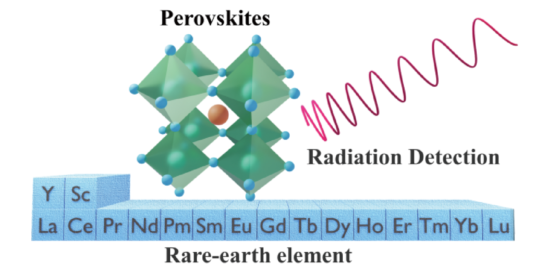
Rare EarthDoped Lead Halide Perovskites: Synthesis, Properties and RadiationDetectors
Received date: 2023-04-07
Revised date: 2023-09-17
Online published: 2023-11-30
Supported by
National Natural Science Foundation of China(12174016)
National Key R&D Program of China(2021YFA1200201)
Beijing Outstanding Young Scientists Projects(BJJWZYJH01201910005018)
Beijing Postdoctoral Research Foundation(Q6009A03202301)
In recent years, lead halide perovskites have shown excellent performance in photovoltaic devices and photodetectors due to its excellent semiconductor properties and have become a hot spot in materials science.Doping rare earth elements is a promising way to improve the performances of lead halide perovskites. In this paper, we review the latest research progress of rare earths doped lead halide perovskite materials in the preparation, structures, properties, as well as radiation detectors. The doped rare earths introduce new luminescent centers and energy levels for new luminescence properties, improving the crystallinity and semiconductor performances of perovskite crystals. Therefore, rare earth doping can further improve the performance of lead halide perovskite radiation detectors.
1 Introduction
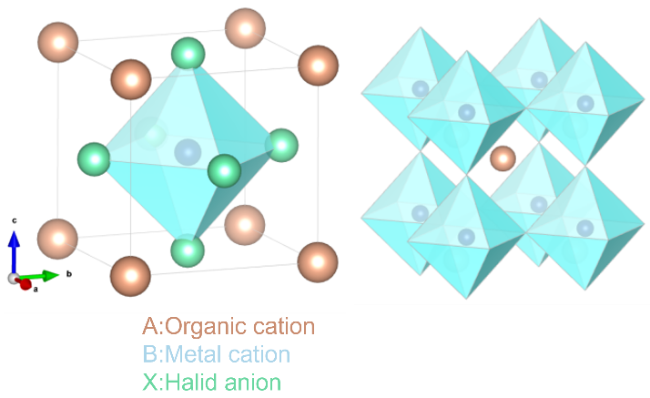
2 Growth and structure of rare earth doped lead halides perovskites
2.1 rare earth ions and Rare earth doped lead halides perovskites
2.2 Synthesis of rare earth-doped lead halides perovskites
2.3 Effect of rare earth ions on the growth and structure of perovskite
2.4 Composition distribution and doping sites of rare earth ions in lead halide perovskite
3 Luminescence properties of rare earth doped lead halides perovskites
3.1 Introducing the luminous centers of rare earth ions
3.2 Enhanced emission of perovskite matrix
4 Semiconductor electrical properties of rare earth doped lead halides perovskites
4.1 Theoretical study on electrical doping of lead perovskite halide by rare earth ions
4.2 Experimental study on electrical doping of lead perovskite halide by rare earth ions
5 Application of rare earth Ions doped lead halides perovskite crystals in radiation detection
5.1 Brief introduction of perovskite radiation detection
5.2 Rare earth doped lead perovskite halide radiation radiation detector
6 Conclusion and prospect
Weiran Chen , Lin Ma , Ting Zhao , Zhengguang Yan , Jiawen Xiao , Zhenzhong Wang , Xiaodong Han . Rare EarthDoped Lead Halide Perovskites: Synthesis, Properties and RadiationDetectors[J]. Progress in Chemistry, 2023 , 35(12) : 1864 -1880 . DOI: 10.7536/PC230404
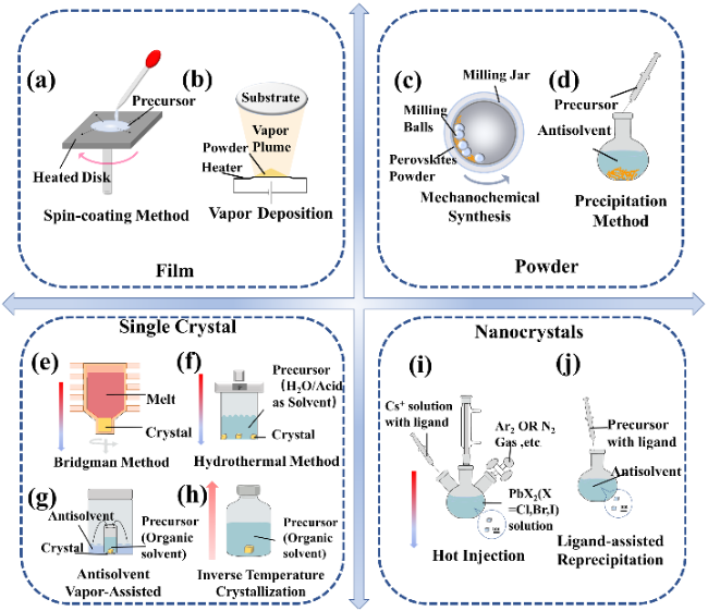
图2 典型的钙钛矿晶体合成手段。 (a) 旋涂法, (b) 气相沉积法, (c) 机械化学研磨法, (d) 沉淀法, (e) 布里奇曼法, (f) 水热法, (g) 反溶剂蒸发辅助结晶法, (h) 逆温结晶法, (i) 热注入法, (j) 配体辅助沉淀法合成纳米晶体Fig. 2 Typical synthesis methods for perovskite crystals. (a) Spin coating method, (b) Vapor deposition method, (c) Mechanochemical synthesis method, (d) Precipitation method, (e) Bridgman method, (f) Hydrothermal method, (g) Antisolvent vapor-assisted method, AVC, (h) Inverse temperature crystallization method, ITC, (i) Thermal injection method, HI, (j) Ligand assisted precipitation method, LARP |
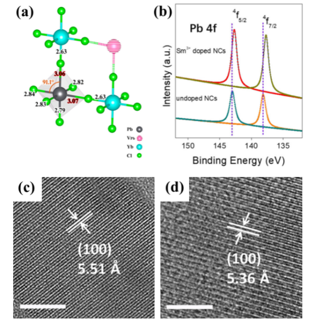
图3 (a) CsPbCl3:Yb3+ 的掺杂局部的晶体结构模型[61]; (b) CsPbCl3:Sm3+纳米晶和无掺杂CsPbCl3纳米晶样品的Pb2+的高分辨XPS谱图[67] ;(c) CsPbCl3:2.1%Yb3+纳米晶与(d) CsPbCl3:5.7%Yb3+纳米晶的HRTEM图像,标尺为5 nm[63]Fig. 3 (a) Crystal structure model of the doped region of CsPbCl3: Yb3+[61]. Copyright 2019, American Chemical Society (b) High-resolution XPS analysis corresponding to Pb4f5/2 and 4f7/2 for undoped and CsPbCl3:Sm3+ NCs[67]. Copyright 2020, American Chemical Society (c) HRTEM images of CsPbCl3:2.1%Yb3+ and (d) CsPbCl3:5.7%Yb3+ NCs.Scale bar: 5 nm[63]. Copyright 2018, American Chemical Society |
表1 稀土掺杂卤化铅钙钛矿的发光性能Table 1 Luminescence properties of lead halide perovskite doped with rare earth |
| Perovskite | Rare-earth Ion | Form of Crystal | Synthesis Mothod | Emisson of Rare-earth ion/Excitation Wavelength(nm) | Emisson of Perovskite as Host (nm) | PLQY (Max) | Response under X-ray | ref |
|---|---|---|---|---|---|---|---|---|
| CsPbCl3 | / | Nano Crystal | Hot-Injection | / | No report | ~54.08% | No report | 88 |
CsPbCl3 | Dy3+ | Single Crystal | Vertical Bridgman | 576.5/455 | No report | 57% | No report | 33 |
| CsPbCl3 | Er3+ | Single Crystal | Vertical Bridgman | 3500/660 4500,2750,1550/800 | No report | No report | No report | 34 |
| CsPbCl3 | Yb3+ | Single Crystal | Vertical Bridgman | 982/375 | 420 | No report | No report | 35 |
| CsPbCl3 | Yb3+ | Single Crystal | Hydrothermal | 980/365 | 450 | 137% | Light yield: 112 000 ph/MeV Detection limit: 176.5 nGyair/s | 89 |
| CsPbCl3 | Yb3+ | Powder | Precipitation | 1000/405 | 406 | No report | Light yield: 102 000 ph/MeV | 24 |
| CsPbCl3 | Y3+ | Nano Crystal | Surface Treatment | / | 404 | 60% | No report | 78 |
| CsPbCl3 | Ce3+, Sm3+, Eu3+, Tb3+,Dy3+, Er3+, Yb3+ | Nano Crystal | Hot Injection | 430 (Ce3+); 560,605,640 (Sm3+); 588,620,696 (Eu3+), 489,550 (Tb3+); 481,572 (Dy3+); 523,548 (Er3+); 982(Yb3+)/365 | 410 | 24.3 (Ce3+); 14.1 (Sm3+); 27.2 (Eu3+); 31.2 (Tb3+); 27.6 (Dy3+); 15.1 (Er3+); 142.7(Yb3+) | No report | 45 |
| CsPb(Br/Cl)3 | Nd3+, Sm3+, Eu3+, Tb3+,Dy3+,Yb3+ | Nano Crystal | Ion Exchange | 890, 1058, 1350 (Nd3+); 564, 600, 650, 710 (Sm3+); 590, 616, 700 (Eu3+); 490, 545, 585, 620 (Tb3+); 475, 575, 660, 750 (Dy3+); 980 (Yb3+)/330 | 410~415 | 2%~3% | No report | 47 |
| CsPb(Cl1-xBrx)3 | Yb3+ | Film | Spin Coated | 990/375 | 490 | 193% | No report | 90 |
| MAPbBr3 | Eu2+ | NanoCrystal | LARP | 440,456/350 | 522 | 90% | No report | 46 |
| MAPbBr3 | Er3+ | Single Crystal | AVC | None/420 | 542 | No report | No report | 39 |
| MAPbI3 | Yb3+,Yb3+/Er+ | Single Crystal | Hydrothermal | 980(Yb3+);980,1540(Yb3+/Er3+)/530 | 830 | No report | Planar Au/MAPbI3/Au for direct detected model: 1.16×10⁶ μC G ·cm-2 (-3 V bias) | 41 |
| NMA2PbBr4 | Eu3+ | Film | Spin Coated | 576, 589, 611, 648, 697 /350 | 389,564 | 9% | No report | 70 |
| PEA2PbCl4 | Eu3+ | Powder | Hot Injection | 592,613/365 | 350 | 83% | No report | 71 |
| PEA2PbBr4 | Yb3+ | Micro Crystal | Hot Injection | 997/340 | 414 | No report | No report | 72 |
| CsPbCl3 | La3+ | Single Crystal | Vertical Bridgman | / | 420 | No report | Weaker luminescence intensity under X-ray | 32 |
| CsPbBr3 | Ce3+ | Nano Crystal | Hot Injection | None/340 | 525 | No report | Light yield: 33 000 ph/MeV spatial resolution :862 nm | 91 |
| CsPbI3 | La3+ | Nano Crystal | Hot Injection | / | 687 | 99.3% | No report | 73 |
| CsPbI3 | Ce3+ | Nano Crystal | Hot Injection | None/365 | 678 | 99% | No report | 74 |
| CsPbBr3 | Ce3+ | Nano Crystal | Hot Injection | None/365 | 510 | 89% | No report | 75 |
| CsPbBr3 | Nd3+ | Nano Crystal | LARP | None/365 | 459 | 90% | No report | 66 |
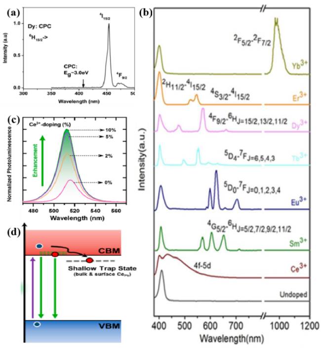
图4 (a) CsPbCl3:Dy3+单晶在575 nm(Dy3+6H15/2 → 4I15/2 )发射波段的激发光谱[33];(b) CsPbCl3:Yb3+/Er3+/Dy3+/Tb3+/Eu3+/Sm3+/Ce3+纳米晶体在365nm激发下的发射光谱[45]; (c) 不同浓度Ce3+ 掺杂CsPbBr3:Ce3+纳米晶体的归一化光致发光光谱; (d) Ce3+掺杂CsPbBr3提出的辐射复合增强模型,灰色虚线代表浅层缺陷能级,绿色虚线代表导带上的额外电子态[76]Fig. 4 (a) Excitation spectra of CsPbCl3:Dy3+ SC at 575nm (Dy3+6H15/2 → 4I15/2 )emission band[33]. Copyright 2020, The Optical Society (b) Emission spectra of CsPbCl3:Yb3+/Er3+/Dy3+/Tb3+/Eu3+/Sm3+/Ce3+ NCs at 365 nm excitation[45]. Copyright 2017, American Chemical Society (c) Normalized PL spectra of CsPbBr3:Ce3+ NCs doping with different concentrations of Ce3+. (d) The luminescence enhancement model of Ce3+ doped CsPbBr3. The gray dotted line represents the shallow defect energy level and the green dotted line represents the additional electronic states in the conduction band[76]. Copyright 2019, American Chemical Society |
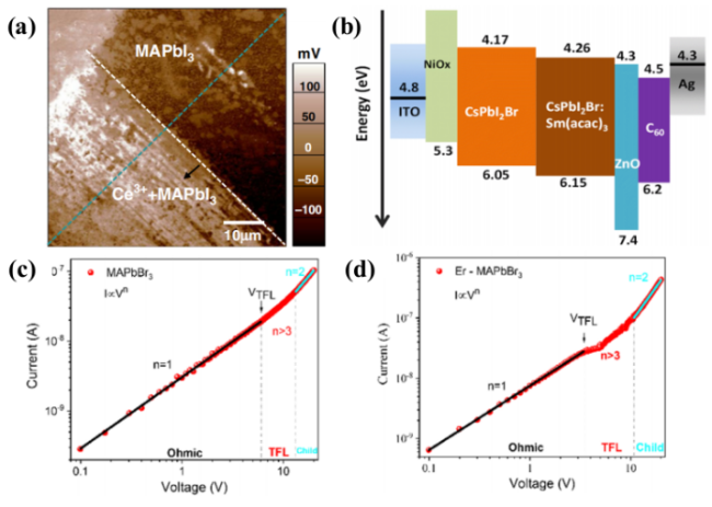
图5 (a) MAPbI3单晶的局部经CeI3颗粒处理后退火后,KPFM下的CPD测量结果[55]; (b) Sm(acac)3掺杂CsPbI2Br太阳能电池的各功能层能带结构图[86]; (c) 无掺杂MAPbBr3单晶与 (d) ErCl3掺杂的MAPbBr3单晶的暗电流电流-电压曲线[39]Fig. 5 (a) CPD measurement via KPFM of MAPbI3 SC partly treat by CeI3 particles followed by followed by thermal annealing[55]. Copyright 2021, Nature Publishing Group (b) The energy band structure diagram of Sm(acac)3-doped CsPbI2Br solar cell[86]. Copyright 2020, AIP Publishing (c) The dark current-voltage curves of undoped MAPbBr3 SC and (d) ErCl3-doped MAPbBr3 SC[39]. Copyright 2020, American Chemical Society |
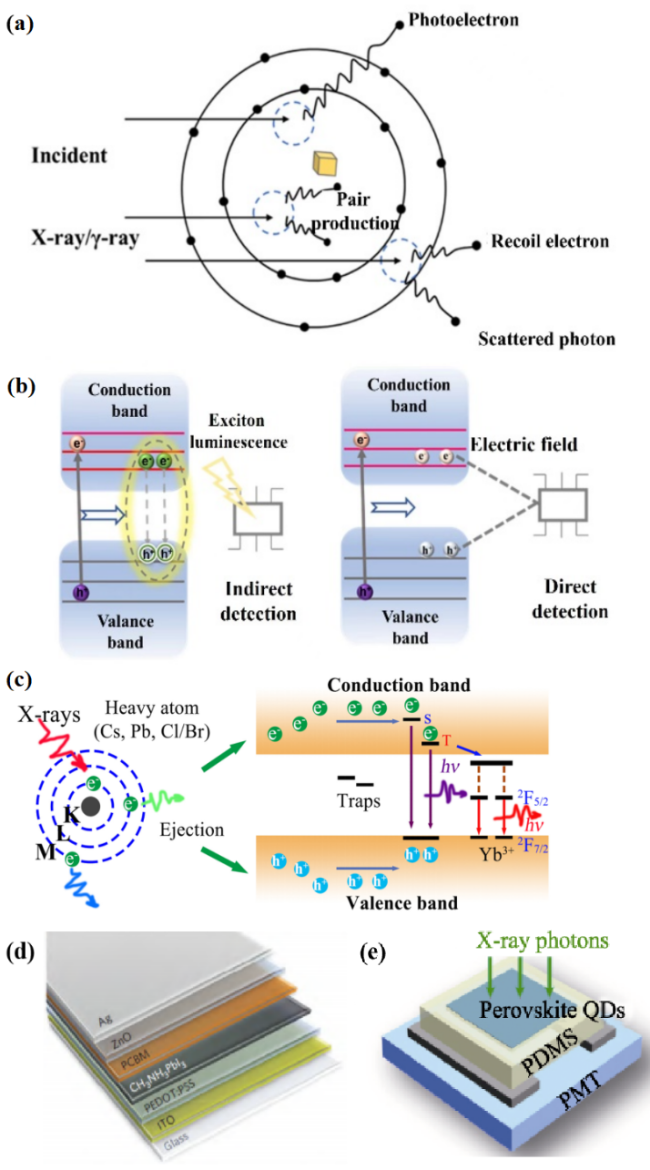
图6 (a) 固体材料吸收射线的主要作用过程机理;(b) 闪烁探测晶体与半导体探测材料的探测原理示意图;(c) CsPbClxBr3-x: Yb3+ SCs中闪烁体转换机理简图[102]; (d) 基于MAPbI3的p-i-n型光伏器件结构图[103]; (e) CsPbBr3闪烁体基射线探测器[104]Fig. 6 (a) The principal mechanism by which radiation is absorbed by solid materials; (b) Schematic diagram of the detection principle of scintillation detection crystals and semiconductor detection materials; (c) A sketch of the scintillators conversion mechanism in CsPbClxBr3-x: Yb3+ SCs[102]; (d) Schematic of layer stacking of the MAPbI3-based p-i-n photodiode[103]; (e) CsPbBr3 scintillator based ray detector[104] |
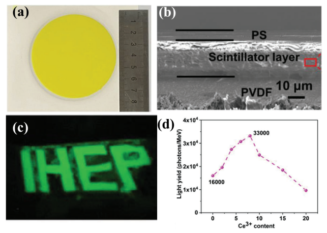
图7 (a) CsPbBr3:Ce3+钙钛矿复合薄膜的光学照片;(b) CsPbBr3:Ce3+钙钛矿复合薄膜的横截面SEM照片;(c) CsPbBr3:Ce3+钙钛矿复合薄膜在X射线下的对LOGO的成像效果;(d) 不同浓度稀土掺杂的CsPbBr3:Ce3+的光产额变化[91]Fig. 7 (a) Optical image of the CsPbBr3:Ce3+scintillator film without protective layer. (b) SEM image of the side of scintillator film. (c) the image effect of CsPbBr3:Ce3+ perovskite composite film on LOGO under X-ray. (d) the light yield changes of rare earth doped CsPbBr3:Ce3+ at different concentrations[91]. Copyright 2022 Wiley-VCH. |
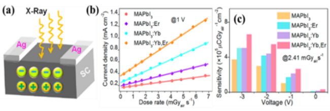
图8 (a) 无掺杂MAPbI3和MAPbI3:RE3+的平面电极X射线探测器件结构图; (b) 1V偏压下无掺杂MAPbI3和MAPbI3:RE3+的光电流强度与辐射剂量率关系; (c) 无掺杂 MAPbI3和MAPbI3: RE3+X射线探测器件的在2.41 mGyair/s剂量下不同偏置电压设定下的灵敏度[41]Fig. 8 (a) Illustration of parallel device structures of undoped MAPbI3 and MAPbI3:RE3+ Single crystals; (b) The relationship between photocurrent intensity and radiation dose rate of undoped MAPbI3 and MAPbI3:RE3+ at 1 V bias; (c) Bias-dependent sensitivity of the detectors at a 2.41 mGyair/s dose rate[41]. Copyright 2020, American Chemical Society |
| [1] |
|
| [2] |
|
| [3] |
|
| [4] |
|
| [5] |
|
| [6] |
|
| [7] |
|
| [8] |
|
| [9] |
|
| [10] |
|
| [11] |
|
| [12] |
|
| [13] |
|
| [14] |
(张思远. 稀土离子的光谱学:光谱性质和光谱理论. 北京: 科学出版社, 2008.).
|
| [15] |
(张胤. 稀土功能材料. 北京: 化学工业出版社, 2015.).
|
| [16] |
(闫业玲, 曹俊媚, 孟凡宁, 王宁, 高立国, 马廷丽. 化学进展, 2019, 31(07): 1031.).
|
| [17] |
|
| [18] |
|
| [19] |
|
| [20] |
(姜峰. 基于离子掺杂全无机钙钛矿的发光特性研究. 硕士学位论文,湖南大学, 2020.).
|
| [21] |
|
| [22] |
|
| [23] |
|
| [24] |
|
| [25] |
|
| [26] |
|
| [27] |
|
| [28] |
ShiD,
|
| [29] |
|
| [30] |
|
| [31] |
|
| [32] |
|
| [33] |
|
| [34] |
|
| [35] |
|
| [36] |
|
| [37] |
|
| [38] |
|
| [39] |
|
| [40] |
|
| [41] |
|
| [42] |
|
| [43] |
|
| [44] |
|
| [45] |
|
| [46] |
|
| [47] |
|
| [48] |
(孙蕊. 吉林大学博士学位论文, 2023.).
|
| [49] |
|
| [50] |
|
| [51] |
|
| [52] |
|
| [53] |
|
| [54] |
|
| [55] |
|
| [56] |
|
| [57] |
|
| [58] |
|
| [59] |
|
| [60] |
|
| [61] |
|
| [62] |
|
| [63] |
|
| [64] |
|
| [65] |
|
| [66] |
|
| [67] |
|
| [68] |
|
| [69] |
|
| [70] |
CortecchiaD,
|
| [71] |
XuD,
|
| [72] |
|
| [73] |
|
| [74] |
|
| [75] |
|
| [76] |
|
| [77] |
|
| [78] |
|
| [79] |
|
| [80] |
|
| [81] |
|
| [82] |
|
| [83] |
|
| [84] |
|
| [85] |
|
| [86] |
|
| [87] |
|
| [88] |
|
| [89] |
|
| [90] |
|
| [91] |
|
| [92] |
|
| [93] |
|
| [94] |
|
| [95] |
|
| [96] |
|
| [97] |
|
| [98] |
|
| [99] |
|
| [100] |
|
| [101] |
|
| [102] |
|
| [103] |
(胡刚舰, 陈琦, 魏薇, 孙仔成, 姚梦楠, 沈亮. 发光学报, 2023, 44(5): 771.).
|
| [104] |
(孟钢, 叶雨琪, 范黎明, 王时茂,
|
| [105] |
|
/
| 〈 |
|
〉 |